Non-Isoelectronic Surfactant Assisted Growth In Inverted Metamorphic Multijunction Solar Cells
a solar cell, metamorphic technology, applied in the direction of semiconductor/solid-state device manufacturing, semiconductor devices, electrical apparatus, etc., can solve the problems of not meeting demand for solar cells to meet the needs of more sophisticated applications, and the number of practical difficulties relating to material selection and fabrication steps
- Summary
- Abstract
- Description
- Claims
- Application Information
AI Technical Summary
Benefits of technology
Problems solved by technology
Method used
Image
Examples
second embodiment
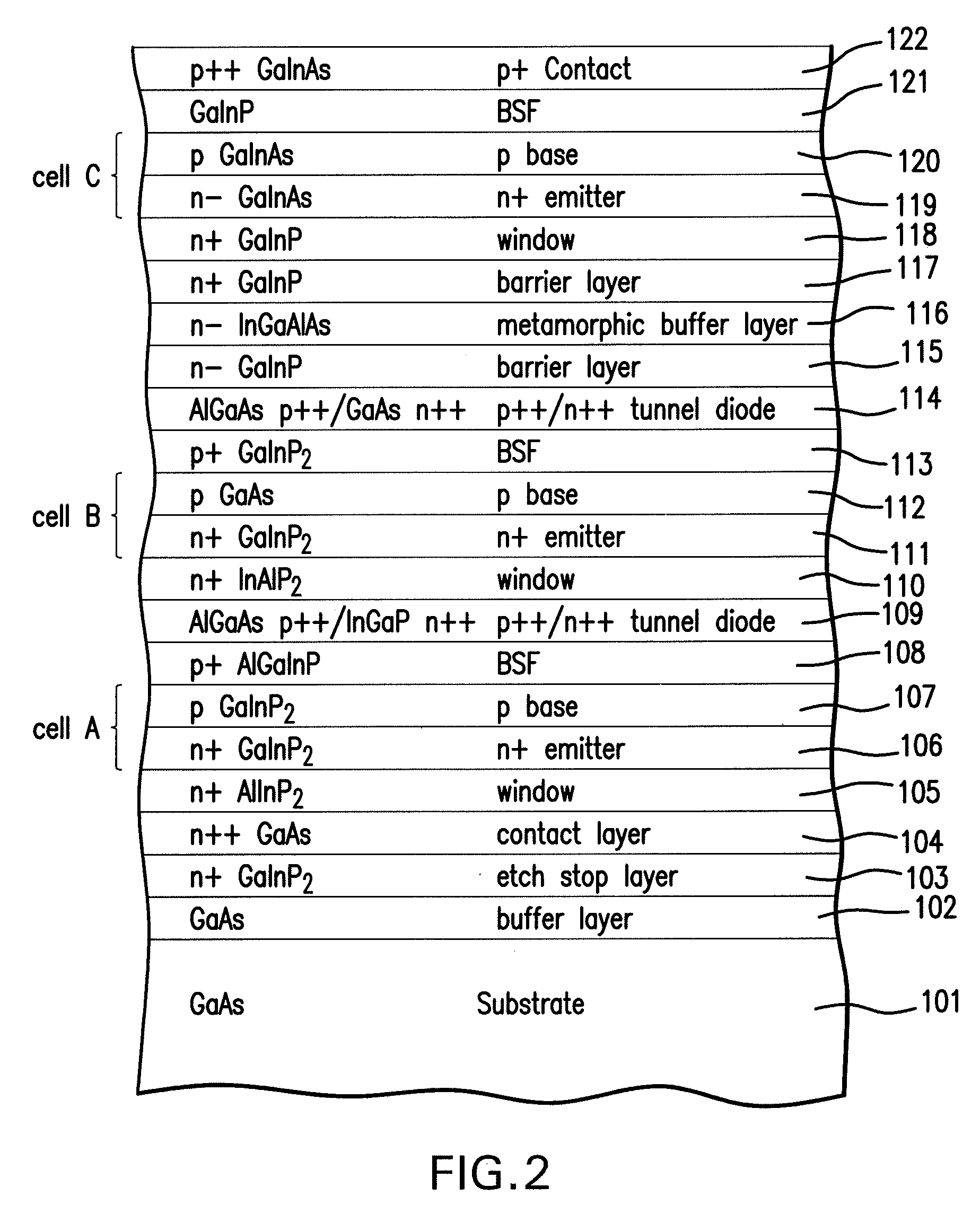
[0067]Although the preferred embodiment of the present invention utilizes a plurality of layers of InGaAlAs for the metamorphic layer 116 for reasons of manufacturability and radiation transparency, other embodiments of the present invention may utilize different material systems to achieve a change in lattice constant from subcell B to subcell C. Thus, the system of Wanlass using compositionally graded InGaP is the present invention. Other embodiments of the present invention may utilize continuously graded, as opposed to step graded, materials. More generally, the graded interlayer may be composed of any of the As, P, N, Sb based III-V compound semiconductors subject to the constraints of having the in-plane lattice parameter greater or equal to that of the second solar cell and less than or equal to that of the third solar cell, and having a bandgap energy greater than that of the second solar cell.
[0068]In another embodiment of the present invention, an optional second barrier l...
first embodiment
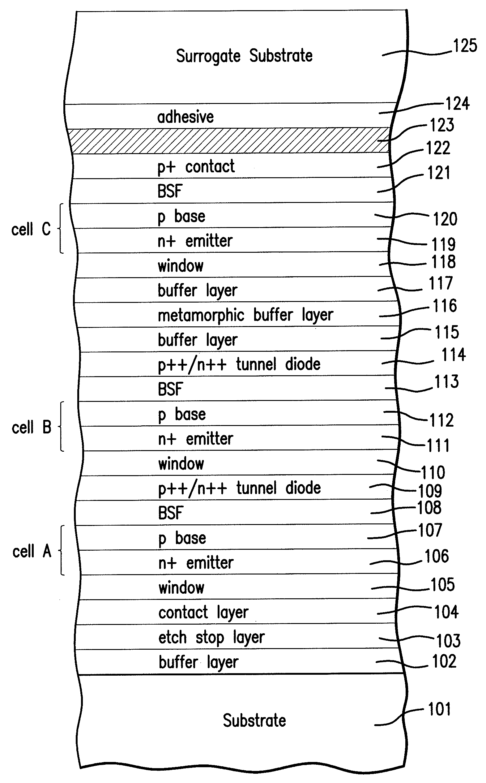
[0088]FIG. 14A is a cross-sectional view of the solar cell of FIG. 12 after the next process step in the present invention in which the surrogate substrate 125 is appropriately thinned to a relatively thin layer 125a, by grinding, lapping, or etching.
[0089]FIG. 14B is a cross-sectional view of the solar cell of FIG. 14A after the next process step in a second embodiment of the present invention in which a cover glass is secured to the top of the cell by an adhesive.
third embodiment
[0090]FIG. 15 is a cross-sectional view of the solar cell of FIG. 14B after the next process step in the present invention in which a cover glass is secured to the top of the cell and the surrogate substrate 125 is entirely removed, leaving only the metal contact layer 123 which forms the backside contact of the solar cell. The surrogate substrate may be reused in subsequent wafer processing operations.
[0091]FIG. 16 is a graph of a doping profile in the emitter and base layers in one or more subcells of the inverted metamorphic multijunction solar cell of the present invention. The various doping profiles within the scope of the present invention, and the advantages of such doping profiles are more particularly described in copending U.S. patent application Ser. No. 11 / 956,069 filed Dec. 13, 2007, herein incorporated by reference. The doping profiles depicted herein are merely illustrative, and other more complex profiles may be utilized as would be apparent to those skilled in the ...
PUM
 Abstract
Description
Claims
Application Information
 - R&D
- Intellectual Property
- Life Sciences
- Materials
- Tech Scout
- Unparalleled Data Quality
- Higher Quality Content
- 60% Fewer Hallucinations
Browse by: Latest US Patents, China's latest patents, Technical Efficacy Thesaurus, Application Domain, Technology Topic, Popular Technical Reports.
© 2025 PatSnap. All rights reserved.Legal|Privacy policy|Modern Slavery Act Transparency Statement|Sitemap|About US| Contact US: help@patsnap.com


