System and method for de-embedding a device under test employing a parametrized netlist

a netlist and device technology, applied in the direction of resistance/reactance/impedence, speed/acceleration/shock measurement, instruments, etc., can solve the problems of significant errors, 4-port network and dut unknown, and pad set introduce significant parasitic effects at high measurement frequency

Inactive Publication Date: 2009-09-10
IBM CORP
View PDF23 Cites 21 Cited by
  • Summary
  • Abstract
  • Description
  • Claims
  • Application Information

AI Technical Summary

Problems solved by technology

Test result obtained from the device test structure includes parasitic effects of the pad set.
In general, the pad set introduces significant parasitic effects at high measurement frequencies.
Unfortunately, the 4-port network and the DUT are unknown.
While the open-short (O-S) de-embedding method provides a simple scheme for estimating the pad set parametrics, the assumption on dominant parametrics and nature of distribution of the pad set parametrics is not true in many cases, and introduces significant errors especially at high frequency, e.g., in GHz frequency ranges and above.
This problem becomes more profound in noise de-embedding particularly in bulk complementary metal-oxide-semiconductor (CMOS) technology, which employs a bulk substrate that induces a large signal loss.
However, use of additional calibration standards to enhance accuracy of the de-embedding increases device characterization cost both by increasing a total test structure area on a semiconductor chip and by increasing the complexity of testing and data analysis.
While benefits of use of increased number of calibration standards are known, the prior art methods also incur significant increase in cost, oftentimes rendering the characterization methods uneconomical.

Method used


Image

  • System and method for de-embedding a device under test employing a parametrized netlist
  • System and method for de-embedding a device under test employing a parametrized netlist
  • System and method for de-embedding a device under test employing a parametrized netlist

Examples


first embodiment

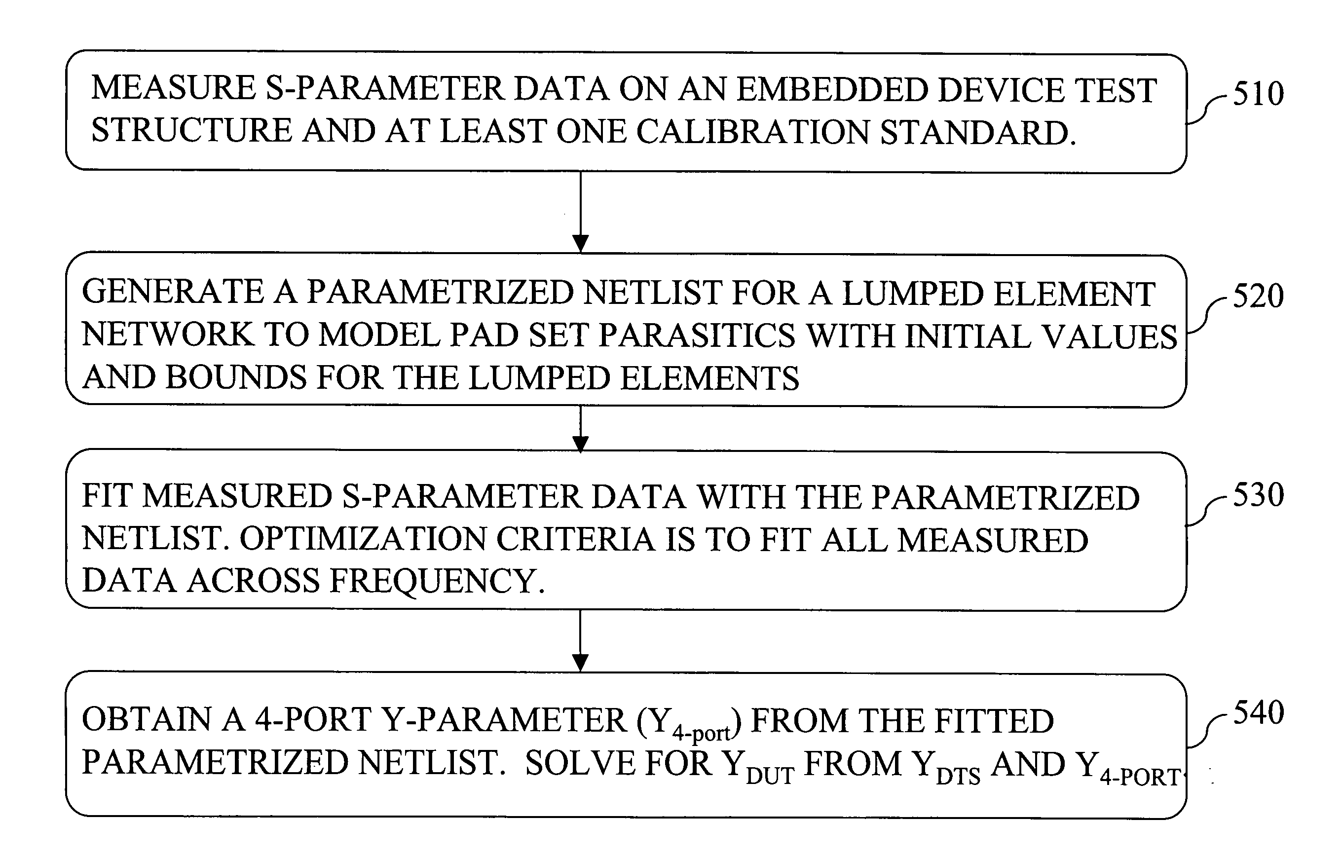
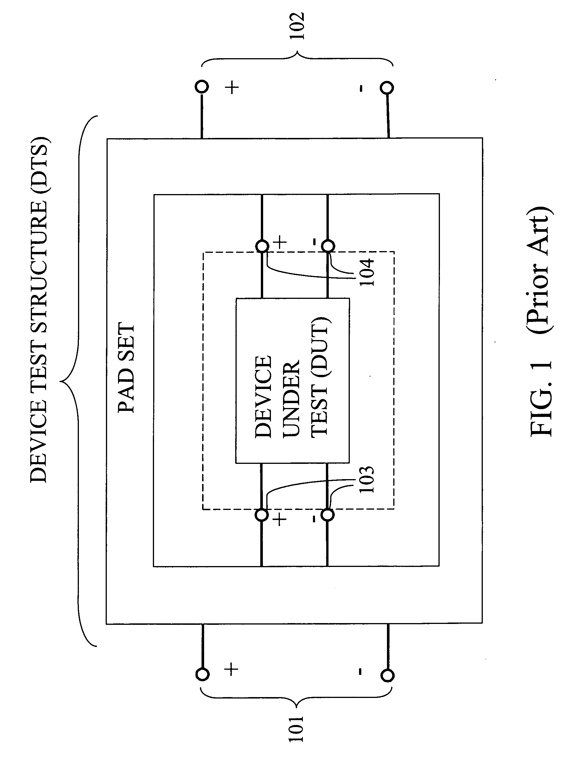
[0088]Referring to FIG. 5, a flow chart illustrating a method for extracting pad set parasitics from a device test structure (DTS) according to the present invention is shown. The DTS embeds a device under test (DUT) and contains a pad set having pad set parasitics that may be modeled with a lumped element model having at least one parameterized lumped element as described above.

[0089]Referring to step 510, scattering parameter (S-parameter) data is measured on the DTS that embeds the DUT. Further, scattering parameter data is also measured on at least one calibration standard, which includes at least one of an open dummy, a short dummy, and a thru dummy. Preferably, the at least one calibration standard includes the open dummy and the short dummy. The S-parameter measurements on the DTS and the at least one calibration standard are performed at multiple frequencies employing a test equipment such as a vector network analyzer (VNA). The measurement frequencies may be at or above 1 G...

second embodiment

[0149]FIG. 6 is a flow chart illustrating a method for extracting a device parameter of a device under test (DUT) embedded in a device test structure (DTS) according to the present invention. Referring to step 610, scattering parameter (S-parameter) data is measured on the DTS that embeds the DUT and on at least one calibration standard as in step 510 of the flow chart in FIG. 5. Preferably, the at least one calibration standard includes the open dummy and the short dummy.

[0150]Referring to step 620, a parametrized netlist containing a lumped element network for the pad set parasitics of the DTS and representing the pad set parasitics of the DTS is generated as in step 520 of FIG. 5, i.e., the parametrized netlist is the same as in the first embodiment of the present invention described above. The parametrized netlist contains a first lumped element network that models the pad set parasitics of the DTS with at least one first parametrized lumped element. The first lumped element net...


PUM


Abstract

S-parameter data is measured on an embedded device test structure, an open dummy, and a short dummy. A 4-port network of the pad set parasitics of the embedded device test structure is modeled by a parameterized netlist containing a lumped element network having at least one parameterized lumped element. The S-parameter data across a range of measurement frequencies is fitted with the parametrized netlist employing the at least one parameterized lumped element as at least one fitting parameter for the S-parameter data. Thus, the fitting method is a multi-frequency fitting for the at least one parameterized lumped element. A 4-port Y-parameter (admittance parameter) is obtained from the fitted parameterized netlist. The Y-parameter of the device under test is obtained from the measured admittance of the embedded device test structure and the calculated 4-port Y parameter.

Description

FIELD OF THE INVENTION[0001]The present invention relates to a system and methods for de-embedding a device under test (DUT) by employing a parametrized netlist having a parameterized lumped element.BACKGROUND OF THE INVENTION[0002]High frequency semiconductor devices are employed to form high frequency semiconductor circuits for communication and / or logic operations. The high frequency semiconductor devices may be a metal-oxide-semiconductor field effect transistor (MOSFET), a bipolar junction transistor (BJT), a passive device such as a capacitor or an inductor, or any other semiconductor device that requires operation at a high frequency, which is typically greater than 1 GHz.[0003]To characterize the high frequency semiconductor devices, high frequency measurements are required. High frequency measurement on a semiconductor device requires a pad set to allow access of a probe, which may be a vector network analyzer (VNA), to the semiconductor device due to microscopic dimensions...

Claims


Application Information

Patent Timeline
Patent Type & Authority Applications(United States)
IPC IPC(8): G01R35/00
CPCG01R35/00G01R27/32
Inventor JAGANNATHAN, BASANTHJIN, ZHENRONGLI, HONGMEI
Owner IBM CORP
Why Eureka
Try Eureka