Electronic device

a technology of electronic devices and electronic components, applied in the direction of cross-talk/noise/interference reduction, line-transmission details, instruments, etc., can solve the problems of insufficient noise countermeasure effects, high radiation noises of in-vehicle electronic devices, and unintended radio waves radiated from printed circuit substrates and power-supply cables, etc., to reduce the common mode current and control unnecessary electromagnetic radiation

Active Publication Date: 2009-08-20
RENESAS ELECTRONICS CORP
View PDF3 Cites 8 Cited by
  • Summary
  • Abstract
  • Description
  • Claims
  • Application Information

AI Technical Summary

Benefits of technology

[0079]It is possible to reduce the common mode current and control the unnecessary electromagnetic radiation.

Problems solved by technology

When electronic devices loaded on vehicles operate, unintended radio waves are radiated from their printed-circuit substrates and power-supply cables (radiation noises).
Due to these radiation noises, reception of radio broadcasting radio waves by on-vehicle antenna is jammed, it is so-called radio noises which has been a serious problem.
However, along with the high-speed of microcomputer's operating frequency in recent years, the radiation noises from in-vehicle electronic devices tend to become high level and high bandwidth.
Therefore, by the conventional stopgap measure like countermeasures, sufficient noise countermeasure effects cannot be attained, and there increased cases which necessitates drastic design changes and increased number of noise countermeasure parts.

Method used


Image

  • Electronic device
  • Electronic device
  • Electronic device

Examples


first embodiment

[0120]In a first embodiment, an example is described where an inductor element is inserted into a power-supply wiring and to correct impedance errors of the power-supply wiring and a GND wiring.

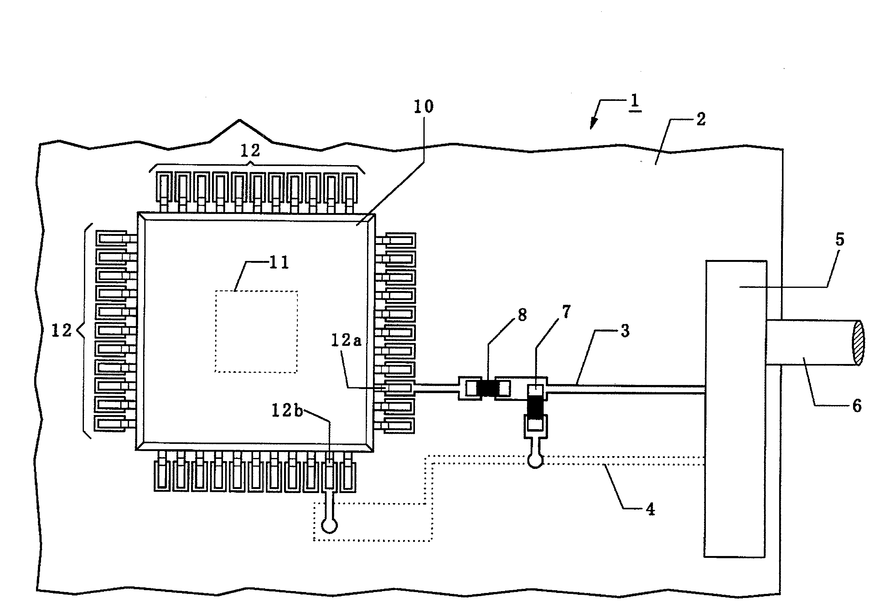
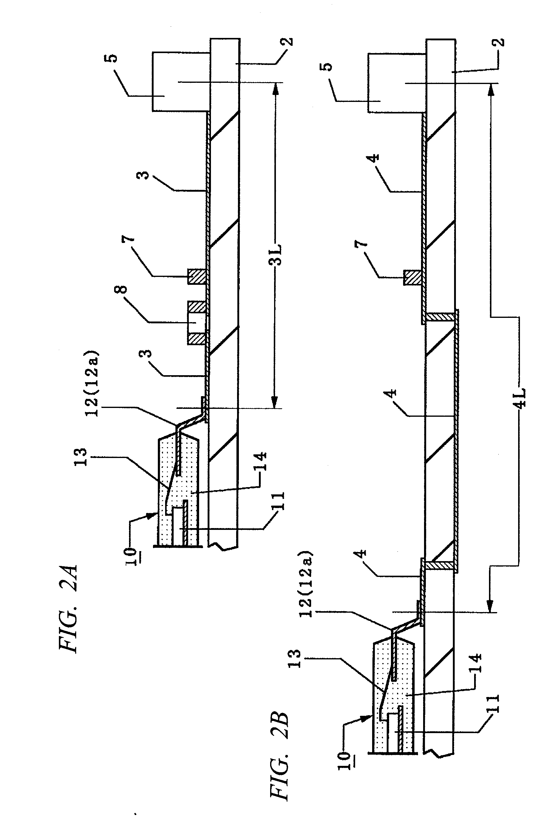
[0121]FIG. 1 and FIG. 2 are diagrams showing an electronic device (electronic device) as the first embodiment according to the present invention, FIG. 1 is a plan view of the electronic device, and FIG. 2 is a cross sectional view of the electronic device (FIG. 2A is a cross sectional view along the power-supply wiring, and FIG. 2B is a cross sectional view along the GND wiring).

[0122]As shown in FIG. 1 and FIG. 2 (FIG. 2A, FIG. 2B), in the electronic device 1 of the first embodiment, as a wiring substrate, on a main surface of, for example, a printed-circuit substrate 2, a connector 5, a capacitor element 7, an inductor element 8, a microcomputer 10 and the like are equipped. As the capacitor element 7 and the inductor element 8, for example ones made of a rectangular surface-mount type (chi...

second embodiment

[0165]FIG. 3 is a plan view showing a schematic structure of an electronic device as a second embodiment according to the present invention.

[0166]In the first embodiment described above, an example where the impedance error of power-supply / GND wirings is corrected by one inductor element 8 has been explained. Meanwhile, as shown in FIG. 3, the impedance error of power-supply / GND wirings may be corrected by two or more inductor elements 8.

third embodiment

[0167]FIG. 4 is a plan view showing a schematic structure of an electronic device as a third embodiment according to the present invention.

[0168]In the first embodiment described above, an example where the inductor element 8 for correcting the impedance error of the power-supply / GND wirings is equipped between the power-supply terminal of the microcomputer 10 and capacitor element 7 has been described. Meanwhile, as shown in FIG. 4, a set of an inductor element 8a and a capacitor element 7a and a set of an inductor element 8b and a capacitor element 7b that correspond to different resonance frequencies may be inserted and loaded so as to widen the frequency band where the effect to reduce the common mode current. For example, the set of the inductor element 8a and the capacitor element 7a is for 48 MHz, and the set of the inductor element 8b and the capacitor element 7b is for 80 MHz.

[0169]In this manner, the inductance element 8 and the capacitor element 7 for correcting impedance...


PUM


Abstract

An electronic device comprising: a wiring substrate having a first power-supply wiring to which a first power-supply potential is applied and a second power-supply wiring to which a second power-supply potential lower than the first power-supply potential is applied; a microcomputer having first and second power-supply terminals in which the first power-supply terminal is connected to the first power-supply wiring and the second power-supply terminal is connected to the second power-supply wiring; and a connector connected to the first and second power-supply wirings, wherein an inductor element for correcting an impedance error of the first and second wirings is connected in series to either one of the first and second power-supply wirings. According to such configuration, unnecessary electromagnetic radiation posed by a common current can be suppressed.

Description

TECHNICAL FIELD[0001]The present invention relates to an electronic device, more particularly, to a technique effectively applied to an electronic device in which a microcomputer is mounted on a wiring substrate thereof as an electronic part.BACKGROUND ART[0002]Along with the advanced computerization and multimedia trends in the society and needs for high functions to information processors, high-speed devices including LSI (Large Scale Integrated Circuit) and memories whose operating frequency exceeds several GHz have been developed continuously. Further, electronic devices have become more compact, and these high-speed devices are packaged in electronic devices at high density. Along with the trends toward high-speed and downsizing, electric noise such as conduction and unnecessary electromagnetic radiation from electronic devices tend to become of high level and high bandwidth. These electric noises not merely cause malfunction in their own circuits, but also cause adverse effect...

Claims


Application Information

Patent Timeline
Patent Type & Authority Applications(United States)
IPC IPC(8): H03H7/00
CPCH05K1/0231H05K1/0233H05K1/165H05K2201/10689H05K2201/1003H05K2201/10189H05K2201/09263H01L2224/48247
Inventor NAKAMURA, ATSUSHIHAYASHI, TORUMABUCHI, YUICHI
Owner RENESAS ELECTRONICS CORP
Why Eureka
Try Eureka