Level shift circuit for a driving circuit

a technology of driving circuit and level shift circuit, which is applied in logic circuits, pulse automatic control, pulse technique, etc., can solve the problems of insufficient “pull low” ability of pull-down transistors, and difficulty in transiting both output signals out and outb from high voltage level vdda, so as to prevent power ground short during transition, enhance transition, and high driving force

Inactive Publication Date: 2009-08-20
HIMAX TECH LTD
View PDF6 Cites 4 Cited by
  • Summary
  • Abstract
  • Description
  • Claims
  • Application Information

AI Technical Summary

Benefits of technology

[0022]The invention provides a level shift circuit. In the level shift circuit, two additional pull-down transistors with high driving force are used for enhancing transition of output signals from H to L while a further transistor is used for preventing power-ground short during transition.

Problems solved by technology

However, accompanied with remarkable advances in semiconductor fabrication process for low power consumption application, VDDD is lower and lower year by year.
So it is difficult to transit both the output signals OUT and OUTB from the high voltage level VDDA into the low voltage level GND, i.e. the “pull low” ability of the pull-down transistors may not enough.

Method used


Image

  • Level shift circuit for a driving circuit
  • Level shift circuit for a driving circuit
  • Level shift circuit for a driving circuit

Examples


Embodiment Construction

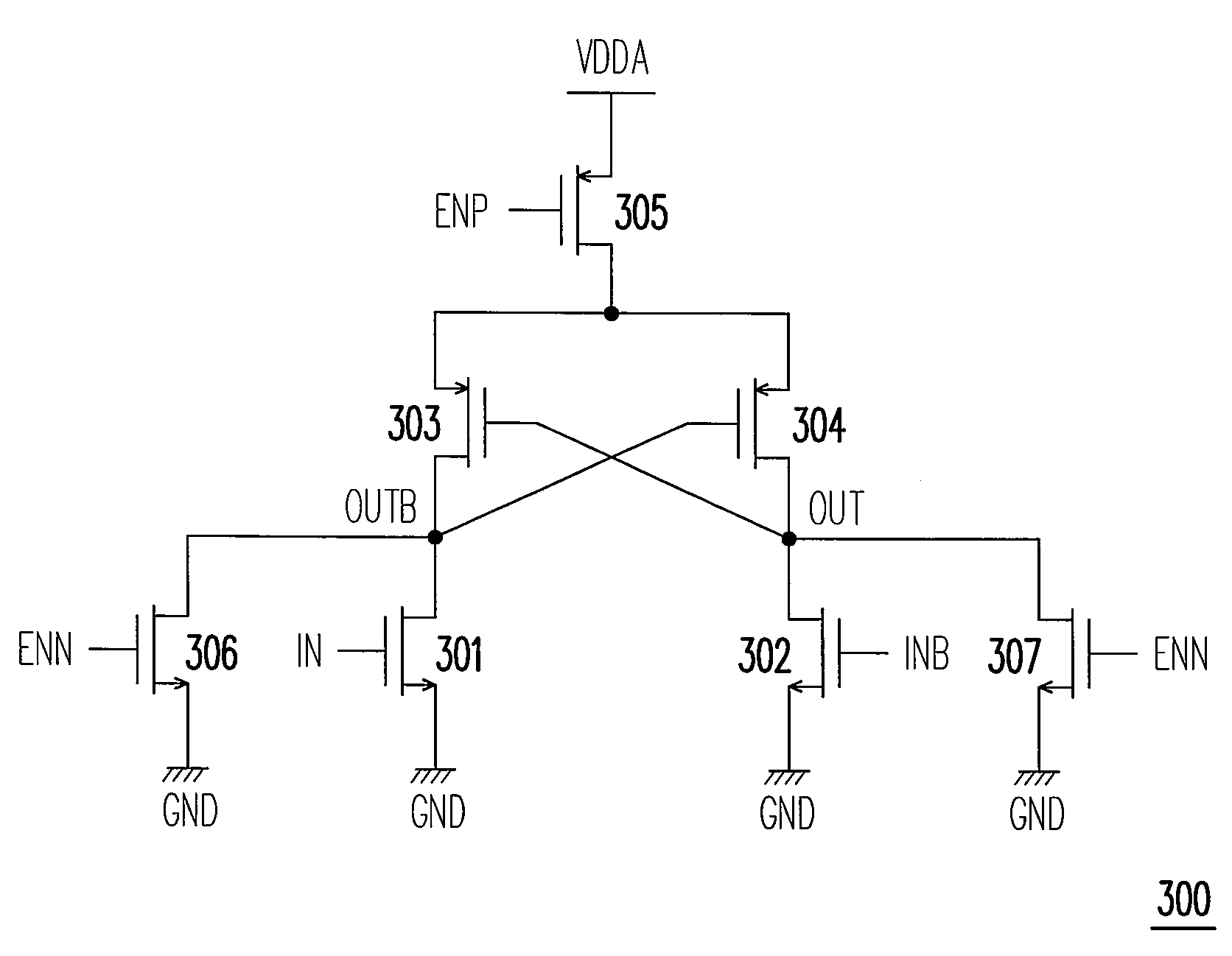
[0039]Reference will now be made in detail to the present embodiments of the invention, examples of which are illustrated in the accompanying drawings. Wherever possible, the same reference numbers are used in the drawings and the description to refer to the same or like parts. The ground terminal GND is not limited to the ground, it may be another power supply voltage VSSA.

[0040]FIG. 5A shows a circuit diagram of a level shift circuit 300 according to an embodiment of the invention. The level shift circuit 300 comprises two pull-down transistors 301 and 302, two pull-up transistors 303 and 304, and three additional transistors 305, 306 and 307.

[0041]The transistor 301 has a source coupled to ground terminal GND, a drain for providing an output signal OUBT, and a gate for receiving an input signal IN.

[0042]The transistor 302 has a source coupled to ground terminal GND, a drain for providing an output signal OUT, and a gate for receiving an input signal INB.

[0043]The transistor 303 h...


PUM


Abstract

Provided is a level shift circuit for a driving circuit. The level shift circuit includes: a cross-coupled transistor pair, for receiving a first input signal and a second input signal and for providing a first output signal and a second output signal; a first transistor, coupled to a first power supply and to the cross-coupled transistor pair, further receiving a first control signal; a second transistor, coupled to the cross-coupled transistor pair and for receiving a second control signal; and a third transistor, coupled to the cross-coupled transistor pair and for receiving the second control signal. The first control signal, the second control signal, the first output signal and the second output signal are all referenced to the first power supply, and the first input signal and the second input signal are referenced to a second power supply lower than the first power supply.

Description

BACKGROUND OF THE INVENTION[0001]1. Field of Invention[0002]The present invention relates to a level shift circuit for a driving circuit.[0003]2. Description of Related Art[0004]Various types of electronic devices have display devices, such as TVs, laptop computers, monitors and mobile communication terminals. The display devices are requested to be thin and / or light in order to save the volume and the cost of the electronic devices. To satisfy these requirements, various Flat Panel Displays (FPDs) have been developed as alternatives to more conventional cathode ray tube displays.[0005]A Liquid Crystal Display (LCD) is one kind of Flat Panel Display. FIG. 1 is a block diagram illustrating functional elements of an LCD device. As illustrated in FIG. 1, an LCD device 2 includes a timing controller 3, a gate driver 4, a LCD panel 5 and a source driving circuit 100.[0006]An image is displayed by applying voltage into the common electrode and the pixel electrode, and then controlling int...

Claims


Application Information

Patent Timeline
Patent Type & Authority Applications(United States)
IPC IPC(8): H03K19/0175
CPCH03K3/356139
Inventor FAN, WEN-TENG
Owner HIMAX TECH LTD
Why Eureka
Try Eureka