Apparatus and method for testing electronic systems

a technology of electronic systems and apparatus, applied in the direction of digital circuit testing, testing circuits, instruments, etc., can solve the problems of increasing effort, reducing the consuming a lot of resources, so as to reduce the required amount of memory on the test chip, reliably validate system behavior, and eliminate redundant or unnecessary test cycles

Inactive Publication Date: 2009-07-30
SALMON PETER C
View PDF83 Cites 4 Cited by
  • Summary
  • Abstract
  • Description
  • Claims
  • Application Information

AI Technical Summary

Benefits of technology

[0011]The test system includes a learn mode and a test mode. The learn mode allows test vectors generated during selected cycles of system behavior to be automatically accumulated in memory. These vectors can be created by a reference system that is hopefully fully functional, or close to fully functional. The cycles selected are test cycles; they capture critical system behaviors or responses. Eliminating redundant or unnecessary test cycles has the benefit of reducing the required amount of memory on the test chip. The test program starts at time=0 with cycle count=0. The cycle count increments with each cycle of the timing reference or system clock. The temporal locations of selected cycles (cycle counts) are captured in a test mask which includes a memory bit for each test cycle performed. A “1” in the mask memory represents a selected cycle for which verification is required (a test cycle); a “0” represents an unselected cycle for which verification is not required. Typically, only a small percentage of total system cycles are required to be test cycles in order to reliably validate system behavior.
[0012]Successive approximations are employed to capture and refine the learned behavior of a properly functioning system. The goal is to automate the process where possible, avoid writing a detailed test program in a software language foreign to the system designers, and reduce the amount of labor required to optimize the selection of effective test vectors. After the learned behavior is refined and verified, the test vectors become proven test vectors; they can be loaded into reference memories for comparison with observed behavior of a system under test (SUT).

Problems solved by technology

To this end, systems have been produced that employ bare IC chips rather than packaged parts, with the IC chips attached to the system board using flip chip bonding methods, resulting in dense systems and short trace lengths.
A lot of effort is required to determine the stimulus vectors and the correct system responses, and the effort increases as system complexity increases.
For some complex systems this approach is abandoned because the time and effort are judged to be too great.
These methods are weak in terms of diagnosing problems, because only system level results are accessible.
Recent test fixtures have included expensive GaAs circuits for increased switching speed and electro-optical receivers for isolation between test circuits.
Despite these efforts, some systems cannot be tested at full speed and others have to compromise on test coverage to keep the test time within reasonable bounds.

Method used


Image

  • Apparatus and method for testing electronic systems
  • Apparatus and method for testing electronic systems
  • Apparatus and method for testing electronic systems

Examples


Embodiment Construction

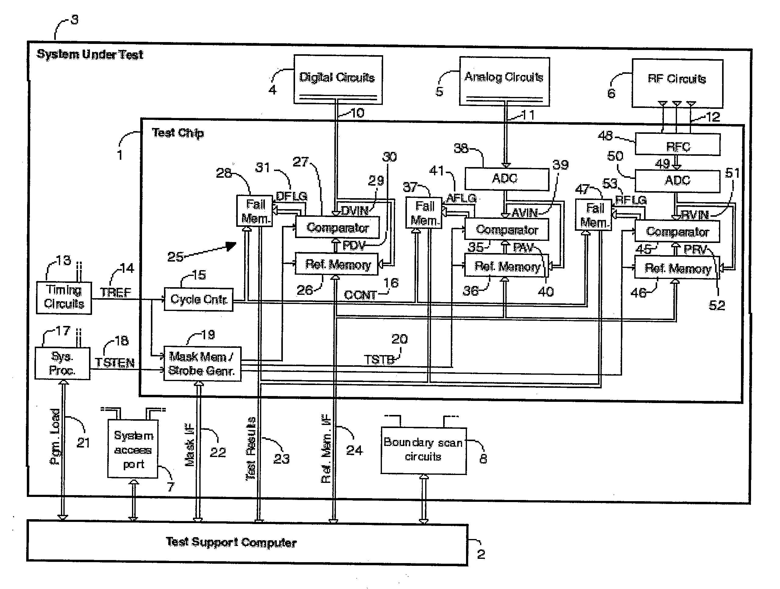
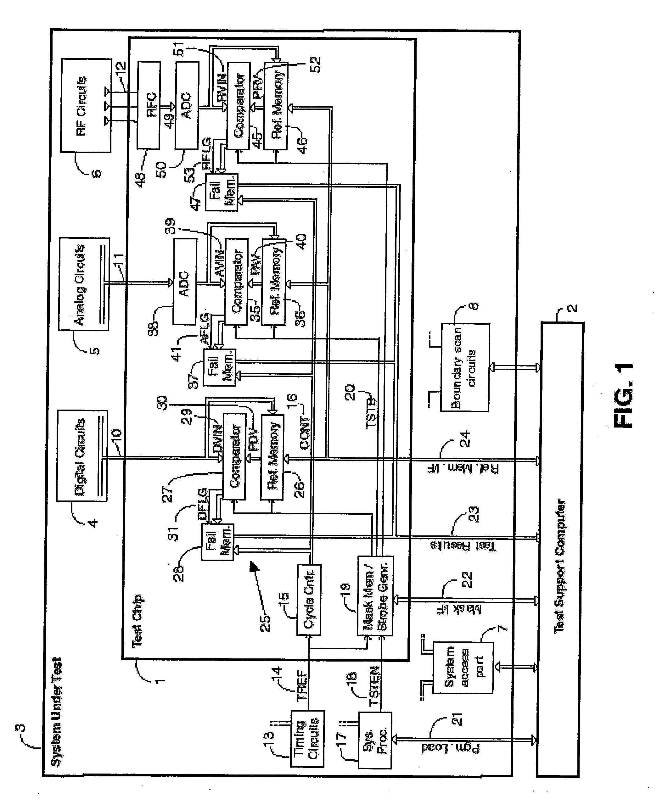
[0017]FIG. 1 shows a high-level block diagram of a test apparatus of the current invention including a test chip 1 and a test support computer 2 connected to the system under test (SUT) 3. SUT 3 includes digital circuits 4, analog circuits 5, and RF circuits 6. System access port 7 is preferably a high-density connection between SUT 3 and test support computer 2. This port is preferably used to validate the interconnection circuits of the SUT using continuity-testing circuits typically provided on a plug-in board within test support computer 2. Similarly, another plug-in board within test support computer 2 may include circuits for testing boundary scan circuits 8 of SUT 3. Plug-in boards can be used for these tests because the clock rates are typically slower than for functional testing; the test hardware is less demanding and is typically available as a commercial-off-the-shelf (COTS) item. Also, connecting wires or cables can be tolerated at the lower test frequencies. In combina...


PUM


Abstract

The technology and economics of system testing have evolved to the point where a radical change in methodology is needed for effective functional testing of systems at clock rates of 1 GHz and higher. Rather than providing a test fixture to interface between the system under test and an external tester, it is preferable to provide critical testing functions within each electronic system in the form of one or more special-purpose test chips. An architecture is proposed that supports full-speed testing with improved noise margins, and also efficient methods for learning correct system behavior and generating the test vectors. The test program is preferably written using the same programming language as used for the system application.

Description

RELATED APPLICATIONS[0001]This application is a continuation of pending U.S. patent application Ser. No. 10 / 448,611 filed May 29, 2003, which claims priority to provisional Application Ser. No. 60 / 452,793 filed Mar. 7, 2003. These applications are each incorporated by reference herein.BRIEF DESCRIPTION OF THE INVENTION[0002]This invention relates to apparatus and method for testing electronic systems, and more particularly to apparatus and method for functionally testing electronic systems at clock rates of 1 GHz and higher.BACKGROUND OF THE INVENTION[0003]Conventional test methods include a hierarchy of tests including wafer probe testing, packaged part testing, and system testing. In each of these, it is customary to use a test fixture between the device under test, DUT, and the tester. The test fixture normally includes a switch matrix for connecting tester pins to DUT pins, and a collection of driver and receiver circuits, switches and relays that are commonly referred to as the...

Claims


Application Information

Patent Timeline
Patent Type & Authority Applications(United States)
IPC IPC(8): G06F19/00G01R31/00G06F15/18G01M99/00G01RG01R31/317G01R31/3187
CPCG01R31/31724G01R31/3187G01R31/31727
Inventor SALMON, PETER C.
Owner SALMON PETER C
Why Eureka
Try Eureka