Flat-panel display member and its manufacturing method and flat-panel display and its manufacturing method
- Summary
- Abstract
- Description
- Claims
- Application Information
AI Technical Summary
Benefits of technology
Problems solved by technology
Method used
Image
Examples
example 1
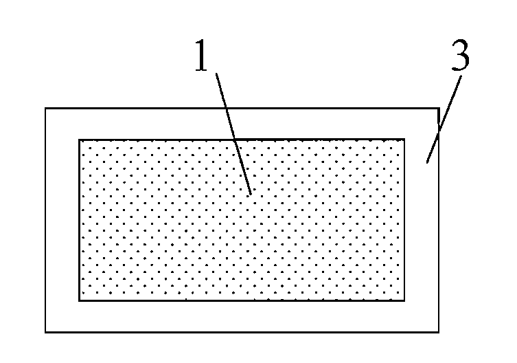
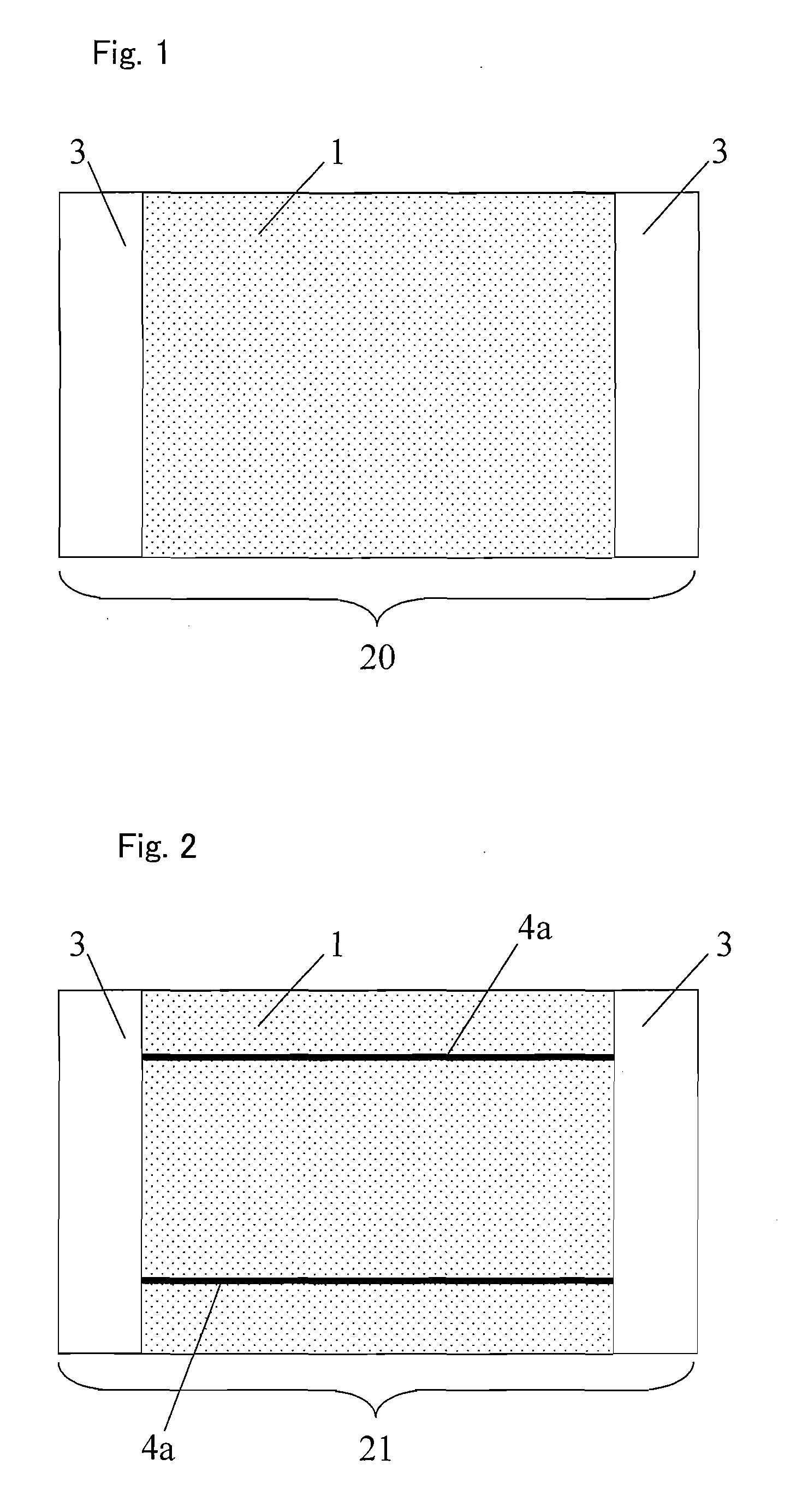
[0211]First, the light detachment processed PET film of a 570×950 mm film-like sticking material was detached, and then the sticking face was affixed to the PET film face of a 570×950 mm anti-reflection film using a sheet laminator, with the positions of the ends being put together, to thereby obtain an anti-reflection film with a sticking material. Next, the heavy detachment processed PET film of the film-like sticking material of the above anti-reflection film with the sticking material was detached and the sticking face was affixed to the copper mesh face of a 570×980 mm copper mesh film by means of a sheet laminator to obtain laminate 1. FIG. 1 is a schematic plan view of laminate 1 of Example 1. The deviations of the end positions of the copper mesh film and the anti-reflection film with the sticking material were each 0.2 mm on the two long sides and each 15 mm on the two short sides in the peripheral portion of laminate 1 of Example 1, and the ends of the two short sides were...
example 2
[0215]A display member was obtained as in Example 1 with the exception that the laser irradiation conditions had an output of 30% and a head speed of 1300 cm / min. FIG. 2 is a schematic plan view of laminate 2 of Example 2; FIG. 5 is a schematic sectional view of a portion in which a cavity is formed in the thickness direction. The cavity was formed from the outermost surface (outermost surface of the first face side) of the anti-reflection film to a PET film (transparent resin layer) of the copper mesh film, and the copper mesh was exposed in all the directions.
[0216]Moreover, FIG. 6 is a schematic sectional view, in the thickness direction, of a portion in which an electrode of the flat-panel display member of Example 2. The electrode was formed from the outermost surface of the anti-reflection film to the PET film of the copper mesh film. In addition, the average value of the width of the electrode at the height position of the outermost surface was 0.60 mm, the average value of t...
example 3
[0217]Laminate 1 was obtained as in Example 1 with the exception that a 570×980 mm anti-reflection film and a 570×980 mm film-like sticking material were used. FIG. 7 is a schematic plan view of laminate 1 of Example 3. The largest value of the deviations at end positions of a copper mesh film and an anti-reflection film with a sticking material in the peripheral portion of laminate 1 of Example 3 was 0.3 mm.
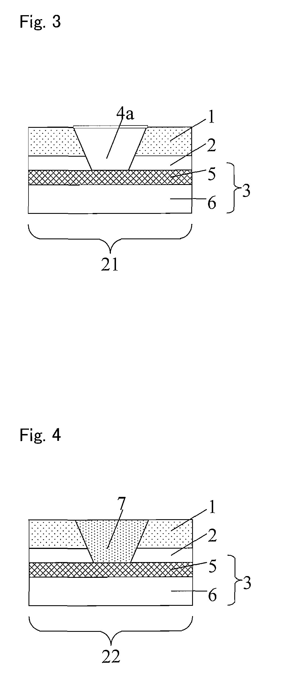
[0218]Next, laminate 1 was fixed to a laser cutter, and cavities were formed in a line shape of lengths of 956 mm in the two long sides and lengths of 546 mm in the two short sides by irradiating 10 mm inside the ends in the peripheral portion of laminate 1 with a laser of an output of 20% and a head speed of 1500 cm / min from the surface of the anti-reflection film of laminate 1 to obtain laminate 2. FIG. 8 is a schematic plan view of laminate 2 of Example 3; FIG. 3 is a schematic sectional view, in the thickness direction, of a portion in which a cavity is formed. The cavity wa...
PUM
 Abstract
Description
Claims
Application Information
 - R&D
- Intellectual Property
- Life Sciences
- Materials
- Tech Scout
- Unparalleled Data Quality
- Higher Quality Content
- 60% Fewer Hallucinations
Browse by: Latest US Patents, China's latest patents, Technical Efficacy Thesaurus, Application Domain, Technology Topic, Popular Technical Reports.
© 2025 PatSnap. All rights reserved.Legal|Privacy policy|Modern Slavery Act Transparency Statement|Sitemap|About US| Contact US: help@patsnap.com


