
Burn-in-board architecture and integrated circuit device transfer method

a technology of integrated circuit devices and design architecture, which is applied in the direction of electronic circuit testing, measurement devices, instruments, etc., can solve the problems of time and space saving, hardware cost, etc., and achieve the effect of reducing physical handling of ic devices, reducing hardware cost, and efficient transfer of a plurality of ic devices

Active Publication Date: 2009-07-09
TEXAS INSTR INC
View PDF4 Cites 12 Cited by
  • Summary
  • Abstract
  • Description
  • Claims
  • Application Information

AI Technical Summary

Benefits of technology

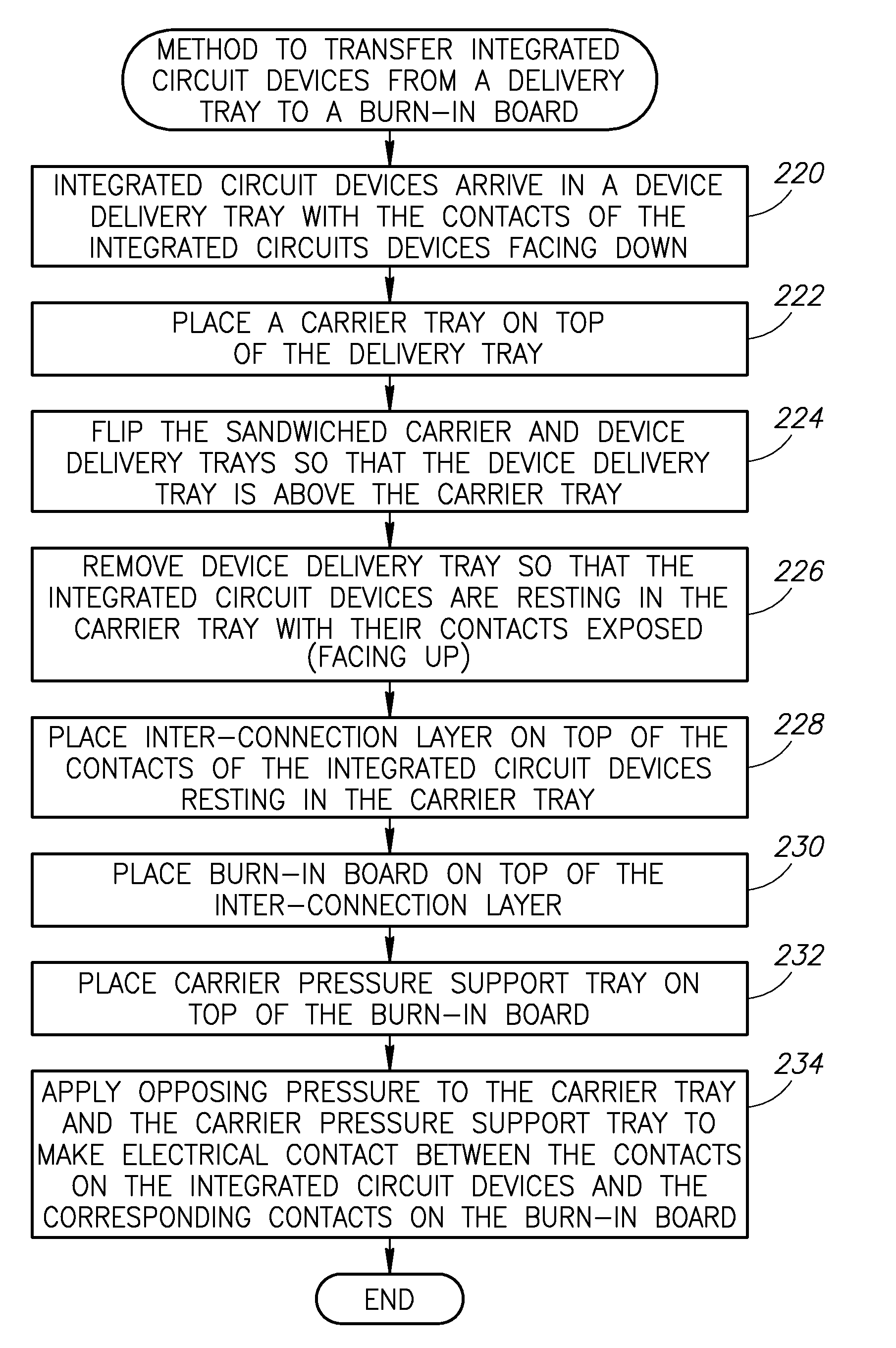
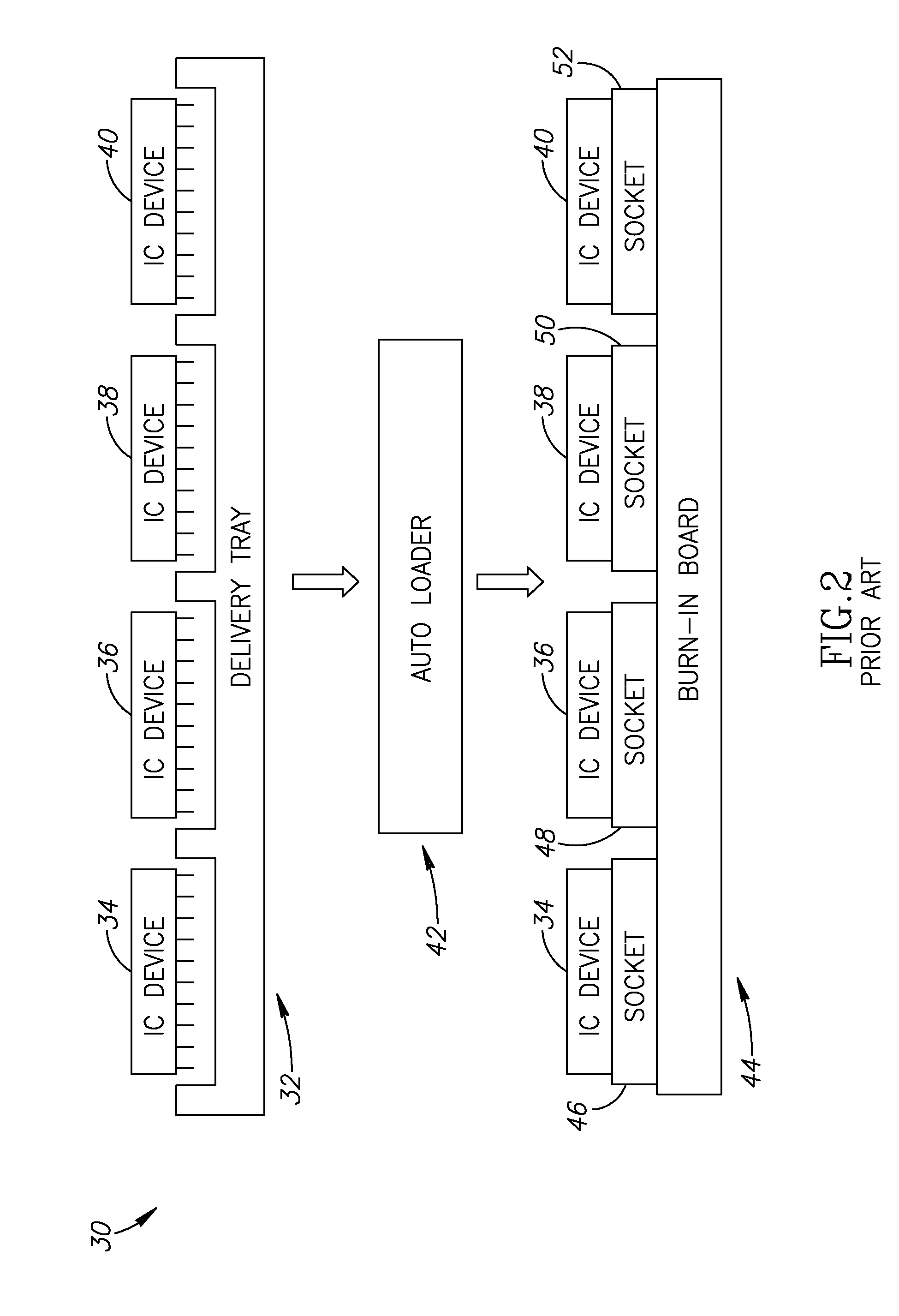
[0010]The present invention also provides a mechanism to efficiently transfer a plurality of IC devices from an IC device delivery tray to a BIB in a single process without using an autoloader as required by the prior art. Eliminating the need for an autoloader results in hardware cost, time and space savings. Transferring all the IC devices from an IC device delivery tray directly to a BIB in a single process reduces the physical handling of the IC devices, and therefore reduces the chance of any potential handling errors.
[0011]The present invention is operative to facilitate the design of BIBs that do not require sockets to hold the IC devices. The absence of sockets facilitates the design of BIBs that are at the same time smaller and hold a greater number of IC devices. The absence of sockets on the BIB, smaller BIB size and increased BIB capacity significantly reduces the cost of manufacturing BIBs. In addition the transferring mechanism of the present invention enables the design of BIBs that hold the same number of IC devices that arrive in the IC device delivery tray. This one to one relationship of IC devices in the IC device delivery tray to IC devices on the BIB adds efficiency to the transfer mechanism of the present invention that was not possible in the prior art.
[0012]Smaller BIBs with greater capacity also enables the design of smaller burn-in ovens that hold a greater number of trays and therefore a greater number of IC devices. This results in cost savings in burn-in oven production (due to smaller size), reduced space requirements and reduced energy requirements.

Problems solved by technology

Eliminating the need for an autoloader results in hardware cost, time and space savings.

Method used


Image

  • Burn-in-board architecture and integrated circuit device transfer method
  • Burn-in-board architecture and integrated circuit device transfer method
  • Burn-in-board architecture and integrated circuit device transfer method

Examples


Embodiment Construction

Notation Used Throughout

[0035]The following notation is used throughout this document.

TermDefinitionBGABall Grid ArrayBIBBurn-In BoardDUTDevice Under TestICIntegrated CircuitPCBPrinted Circuit BoardQFNQuad Flat Leadless PackQFPQuad Flat Pack

Detailed Description of the Invention

[0036]The present invention provides a solution to the prior art problems discussed supra by using an inter-connection layer to couple a plurality of integrated circuit (IC) devices to a burn-in board (BIB), a specific type of printed circuit board used during the burn-in process. The inter-connection layer is comprised of electrical conducting material embedded in a sheet of insulating elastomer (a non-conducting material). When pressure is applied to the inter-connection layer, the embedded electrical conducting material within the inter-connection layer couple to the IC device contacts on one side of the inter-connection layer and the appropriate BIB contacts on the other side of the inter-connection layer....


PUM


Abstract

The present invention implements a mechanism using an inter-connection layer to couple a plurality of integrated circuit devices to a printed circuit board, thereby eliminating the need for sockets to hold the integrated circuit devices on the printed circuit board. The mechanism of the present invention is operative for integrated circuit devices packaged in a ball grid array, a quad flat pack or a leadless quad flat pack. The present invention also provides a mechanism to efficiently transfer a plurality of integrated circuit devices from an integrated circuit device delivery tray to a burn-in board in a single process without requiring an autoloader, resulting in increased transfer reliability and both cost and space savings.

Description

FIELD OF THE INVENTION[0001]The present invention relates to the field of burn-in-board design architecture and more particularly relates to a more efficient method of burn-in-board design which enables a more efficient transfer of a plurality of integrated circuit devices from an integrated circuit device delivery tray to a burn-in board.BACKGROUND OF THE INVENTION[0002]During the integrated circuit (IC) device manufacturing process, a specific percentage of IC devices are subject to a series of testing phases after the silicon dies are attached and electrically to printed circuit boards, thereby creating the IC devices. One of the final testing phases is burn-in, during which the internal core logic of the IC devices are exposed to heat and simultaneously activated with voltage levels that are significantly greater than design specifications. Burn-in typically last several hours at temperatures reaching 140° C. and voltage levels that are typically 40% higher than the IC device de...

Claims


Application Information

Patent Timeline
IPC IPC(8): G01R31/26
CPCG01R31/2863
Inventor WEINRAUB, CHANANIELAMOTZ, EINAM
Owner TEXAS INSTR INC
Learn More