
Multi-band focal plane array

a focal plane array and multi-band technology, applied in the field of focal plane arrays, can solve the problems of limited infrared range of single focal plane array, many of these detectors are only operable, and achieve the effect of improving resolution and enhancing detection resolution

Active Publication Date: 2009-07-09
NORTHROP GRUMMAN SYST CORP
View PDF10 Cites 24 Cited by
  • Summary
  • Abstract
  • Description
  • Claims
  • Application Information

AI Technical Summary

Benefits of technology

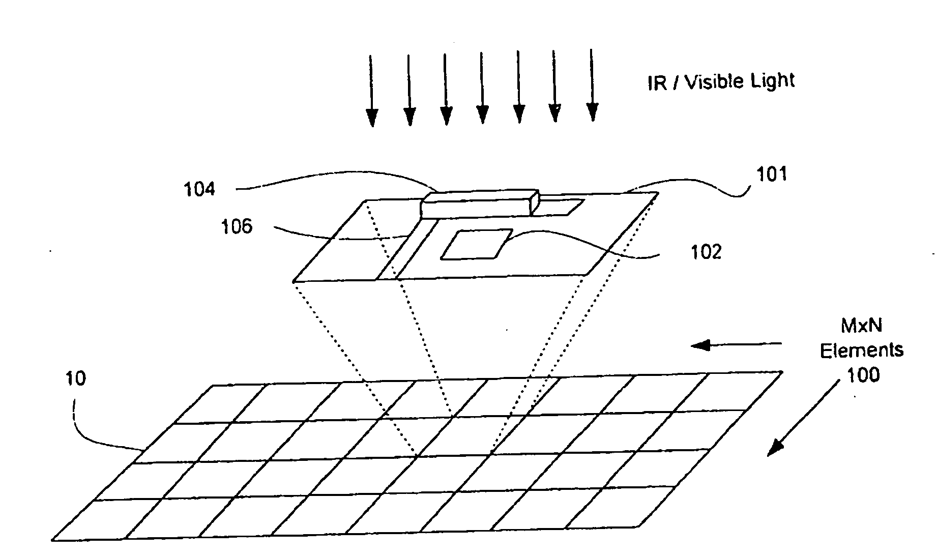
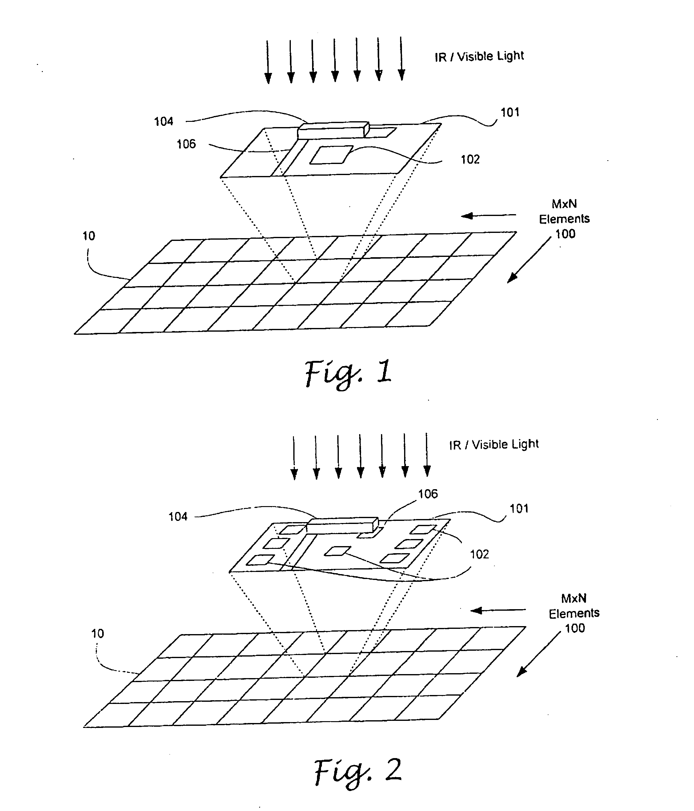
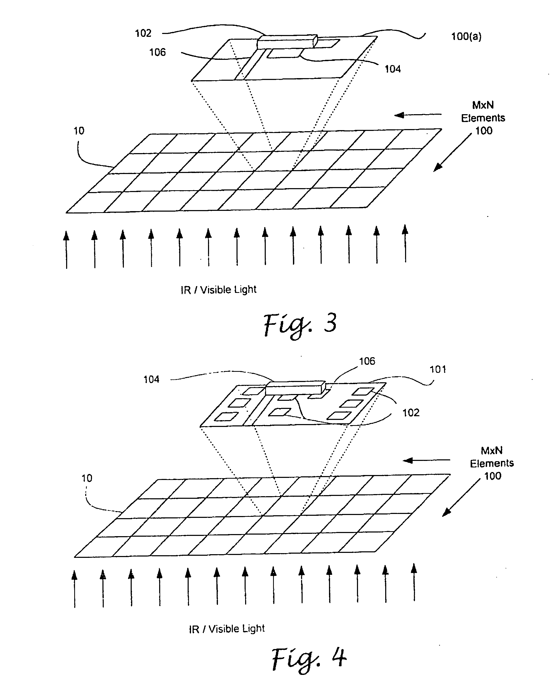
[0007]The focal plane array architecture as provided includes an M×N array of detector elements each having a substrate with a built-in readout circuit, at least one first detector integrated in the substrate at a first side thereof, and a second detector deposited on the first side of the substrate. The first detector includes a visible detector such as a CMOS detector or a CCD detector, while the second detector includes an IR detector operative to detect short or medium wavelength infrared light. When the first detector and the second detector are arranged side by side on the substrate, light at the visible range and the IR range incident on the substrate at the first side thereof, though being detected simultaneously, are not coincident. When the first detector and the second detector are vertically aligned with each other, light at the visible range and the IR range incident on the substrate at a second side opposite to the first side are expected to penetrate through the substrate and incident on the first detector. As the visible detector is transmissive to the IR wavelength range, the light will transmit through the visible detector and incident on the IR detector. Thereby, the visible light and the IR wavelength are coincident to the first and second detectors. In one embodiment, each of the detector elements may includes more than one visible detector to enhance the resolution of the detection in the visible wavelength range.
[0008]In the embodiment comprising two integrated readout circuits flip-chip bonded to each other, at least one array of detectors may be deposited on or integrated in each integrated readout circuit. When each of the integrated readout circuits comprises exactly one array of detectors operative to detect light at two different wavelength bands, a dual-band focal plane array is provided. The array of detectors can also be selected to detect the same wavelength bands of light with an improved resolution. In one embodiment, when one of the integrated readout circuits incorporates more than one array of detectors, detection at three different wavebands can be achieved.

Problems solved by technology

Currently, simultaneous multi-band detection for a single focal plane array is still limited within the infrared range, that is, many of the currently available detectors are only operative to perform simultaneous detection at long-wavelength infrared (LWIR), medium-wavelength infrared (MWIR), and short-wavelength infrared (SWIR) bands.
In addition, many of these detectors are only operable while being cryogenically cooled.

Method used


Image

  • Multi-band focal plane array
  • Multi-band focal plane array
  • Multi-band focal plane array

Examples


Embodiment Construction

[0018]FIG. 1 shows a perspective view of dual-band focal plane array architecture in the form of a silicon-based readout integrated circuit (Si ROIC) 10 partitioned into an M×N array of Si-based readout elements 100, where M and N can be any positive integer. Each of the Si-based readout elements 100 further includes a silicon substrate 101 in which a readout integrated circuit and interconnection are formed (not shown), a visible detector 102, an IR detector 104, and a metal bus 106 for buffering an IR signal generated by the IR detector 104. As silicon is transmissive past 1.1 microns up to about 9 microns and operative to absorb light below 1.1 microns; while such light properties of silicon are not or are only slightly affected doping in the predefined wavebands, the visible detector 102 can be integrated in the form of Si CMOS detector in substrate 101 and fabricated by using any p-n junction available in the CMOS process. Depending on the desired waveband, the IR detector 104 ...


PUM


Abstract

A multi-band focal plane array architecture operative to detect multiple spectral image. The multi-band focal plane array architecture has an integrated readout circuit, a plurality of first detectors integrated in the readout circuit and a plurality of second detectors deposited on the readout circuit. Preferably, the first detectors are operative to detect visible signals and the second detectors are operative to detect infrared signals. The first and second detectors are arranged in a checkerboard pattern, in alternate rows or columns, or at least partially overlapped with each other to realize simultaneous detection in two different wavelength bands. The architecture may also have an additional integrated readout circuit flip-chip bonded to the integrated readout circuit. By forming a plurality of third detectors on the additional integrated readout circuit, a tri-band focal plane array may be realized. In one embodiment, a dual-band focal plane array architecture by forming two arrays of detectors on two individual integrated readout circuit and flip-chip bonding these two readout circuits.

Description

CROSS-REFERENCE TO RELATED APPLICATIONS[0001]Not ApplicableSTATEMENT RE: FEDERALLY SPONSORED RESEARCH / DEVELOPMENT[0002]Not ApplicableBACKGROUND[0003]The present invention relates in generally to a focal plane array, and more particularly, to a multi-band focal plane array (FPA) architecture.[0004]The military has multiple needs for day and night surveillance and reconnaissance. The ultimate goal of an optical imaging sensor is to achieve a high probability of detection of a target while simultaneously maintaining an acceptably low false alarm rate. As a target has a spectral reflectivity or emissivity that varies from the background or from clutter, it is often desirable to detect light from the target in two or more wavebands. Thereby, the target can be detected using the response in the two or three wavebands compared to the response of the focal plane array to the background or clutter in these wavebands. It is also desirable for performing target discrimination in one focal plan...

Claims


Application Information

Patent Timeline
Patent Type & Authority Applications(United States)
IPC IPC(8): H01L27/14H01L27/00
CPCH01L27/14649G01J3/36
Inventor KAUFFMAN, CHRISTOPHER LEEGRIFFITH, GERALD PRAYJONES, RONALD B.YOO, SUNG-SHIKDAVIS, MICHAEL A.
Owner NORTHROP GRUMMAN SYST CORP
Learn More