Method of manufacturing liquid ejection head
a technology of liquid ejection head and liquid ejection head, which is applied in the direction of microlithography exposure apparatus, instruments, photomechanical treatment, etc., can solve the problems of low reproducibility, low reproducibility of circular discharge ports, so as to improve the discharge port and high reproducibility
- Summary
- Abstract
- Description
- Claims
- Application Information
AI Technical Summary
Benefits of technology
Problems solved by technology
Method used
Image

Examples
example 1
[0080]An inkjet-recording head substantially identical to that shown in FIG. 2A was prepared by the manufacturing method described above with reference to FIGS. 3A to 3G.
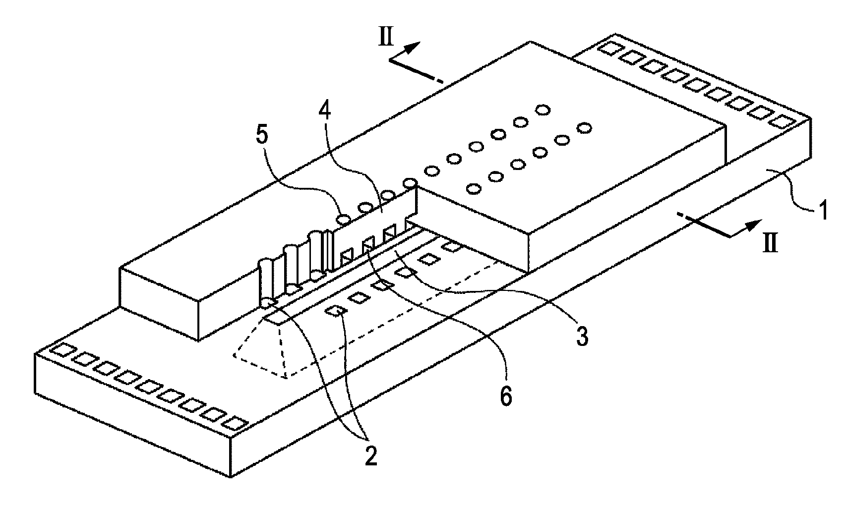
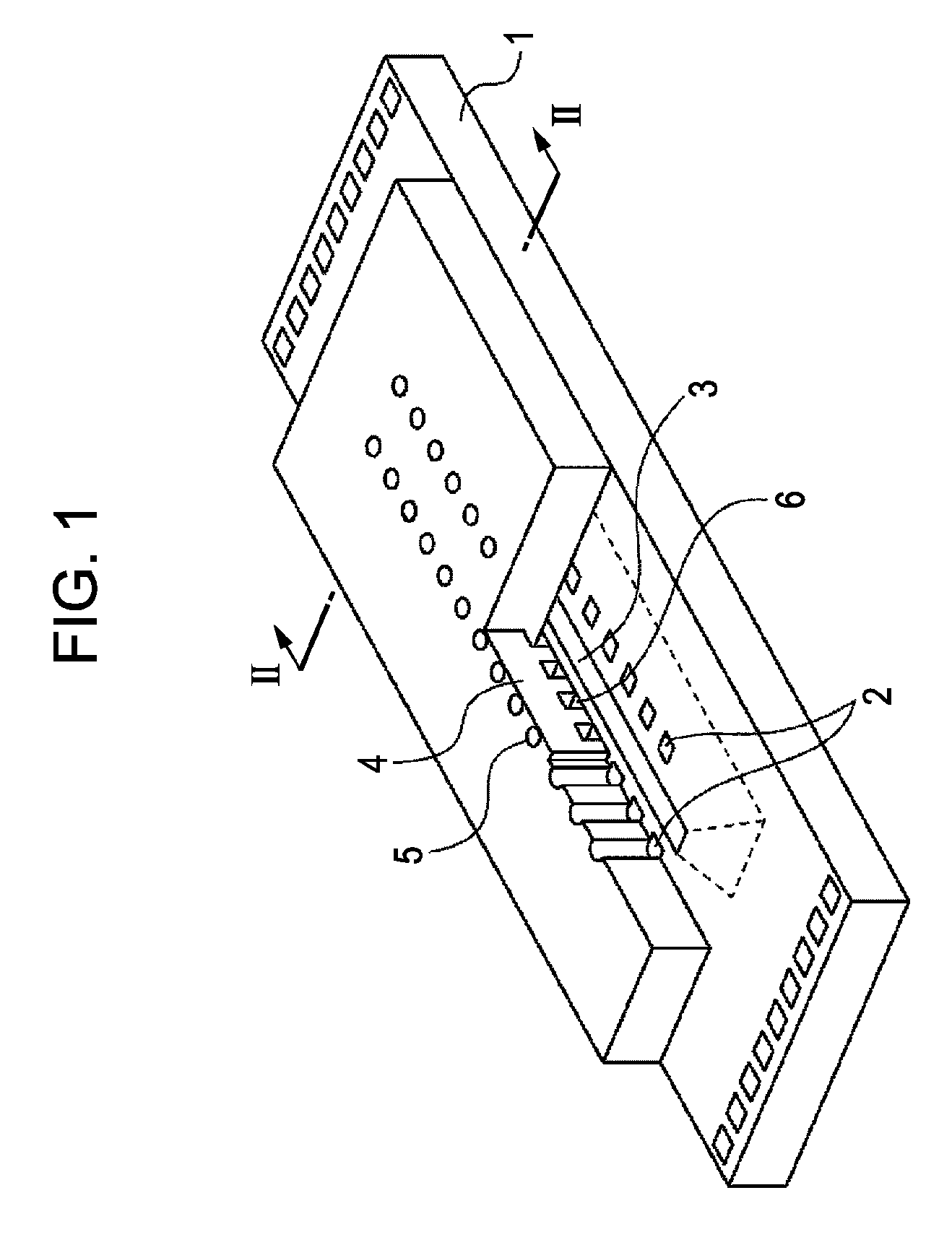
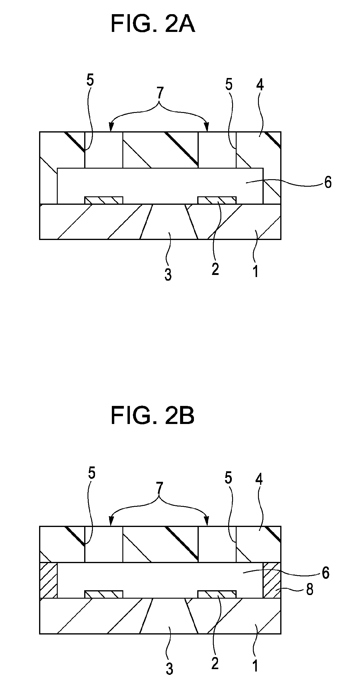
[0081]As shown in FIG. 3A, a substrate 1, made of silicon, having the following components was prepared: electrothermal transducers (heaters made of HfB2) serving as energy-generating elements 2 and a multilayer film (not shown), including a silicon nitride layer and a tantalum layer, for forming an ink channel.
[0082]As shown in FIG. 3B, a layer of a solution prepared by dissolving a first resin composition shown in Table 1 in a solvent was formed on the substrate 1 by spin coating and then baked at 150° C. for three minutes, whereby a positive-type photosensitive resin layer 9 was formed. The positive-type photosensitive resin layer 9 disposed on the substrate 1 had a thickness of 10 μm.
[0083]As shown in FIG. 3C, the positive-type photosensitive resin layer 9 was patterned in such a manner that the positive-type ph...
example 2
[0089]An inkjet-recording head was prepared in substantially the same manner as that described in Example 1 except that a second resin composition shown in Table 1 was used to form a positive-type photosensitive resin layer 9 for forming a pattern 10.
example 3
[0093]Example 3 of the present invention is described below with reference to FIGS. 4A to 4I.
[0094]As shown in FIG. 4A, a substrate 1 substantially identical to that used in Example 1 was prepared.
[0095]A layer of polymethyl isopropenyl ketone, ODUR, available from Tokyo Ohka Kogyo Co., Ltd. was formed on the substrate 1 by spin coating and then baked at 150° C. for three minutes, whereby a first positive-type photosensitive resin layer 9a was formed.
[0096]As shown in FIG. 4C, a layer of a solution prepared by dissolving a third resin composition shown in Table 1 in a solvent was formed on the substrate 1 by spin coating and then baked at 150° C. for three minutes, whereby a second positive-type photosensitive resin layer 9b was formed. The first positive-type photosensitive resin layer 9a had a thickness of 10 μm and the second positive-type photosensitive resin layer 9b had a thickness of 5 μm.
[0097]As shown in FIG. 4D, the second positive-type photosensitive resin layer 9b was pa...
PUM
| Property | Measurement | Unit |
|---|---|---|
| thickness | aaaaa | aaaaa |
| thickness | aaaaa | aaaaa |
| wavelength | aaaaa | aaaaa |
Abstract
Description
Claims
Application Information
 - R&D
- Intellectual Property
- Life Sciences
- Materials
- Tech Scout
- Unparalleled Data Quality
- Higher Quality Content
- 60% Fewer Hallucinations
Browse by: Latest US Patents, China's latest patents, Technical Efficacy Thesaurus, Application Domain, Technology Topic, Popular Technical Reports.
© 2025 PatSnap. All rights reserved.Legal|Privacy policy|Modern Slavery Act Transparency Statement|Sitemap|About US| Contact US: help@patsnap.com