
Si trench between bitline hdp for bvdss improvement

a technology of hdp and bitline, applied in semiconductor devices, semiconductor/solid-state device details, electrical apparatus, etc., can solve the problems of increasing the current between the bitline and the bitline, increasing and affecting the performance of the bvdss, so as to improve the bvdss characteristics, prevent and/or mitigate the leakage of bitline to bitlin

Active Publication Date: 2009-06-18
INFINEON TECH LLC
View PDF3 Cites 3 Cited by
  • Summary
  • Abstract
  • Description
  • Claims
  • Application Information

AI Technical Summary

Benefits of technology

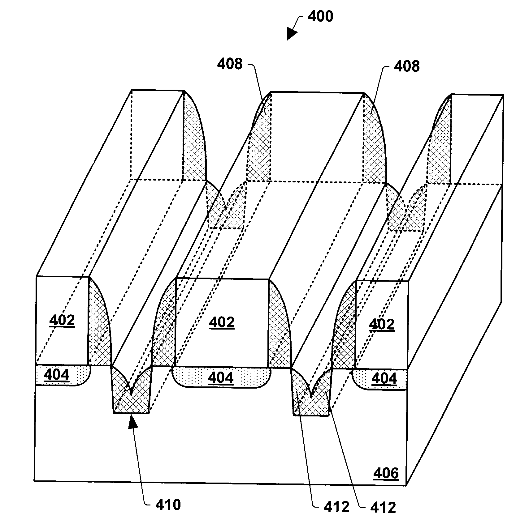
[0007]Another aspect of the subject invention provides methods of making memory devices having improved BVdss characteristics. The methods include forming first spacers adjacent side surfaces of bitline dielectrics and on an upper surface of a semiconductor substrate; forming a trench in the semiconductor substrate between the first spacers; and forming second spacers adjacent the side surfaces of the trench. By containing the trench and the first and second spacers between the bitlines, the memory devices and the methods of making the memory devices can improve the electrical isolation between the bitlines, thereby preventing and / or mitigating bitline-to-bitline current leakage and increasing BVdss.

Problems solved by technology

However, as scaling down device dimensions, bitline-to-bitline leakage may undesirably increase.
Further, bitline contact misalignment may increase leakage current between the bitline and substrate silicon areas adjacent to the bitlines.
However, the increased bitline diffusion region may increase bitline-to-bitline leakage by decreasing the distance between bitlines.

Method used


Image

  • Si trench between bitline hdp for bvdss improvement
  • Si trench between bitline hdp for bvdss improvement
  • Si trench between bitline hdp for bvdss improvement

Examples


Embodiment Construction

[0018]A memory cell, for example, a single bit memory cell or a dual bit memory cell, is programmed by applying a relatively high programming voltage to a control gate and connecting a source to ground and a drain to a predetermined potential above the source. During this process, hot electrons in a core cell channel region near drain inject into the charge storage layer and become trapped since the charge storage layer is electrically isolated from control gate and substrate. As a result of the trapped electrons, the threshold voltage of the cell increases. This change in the threshold voltage (and thereby the channel conductance) of the cell created by the trapped electrons is what causes the cell to be programmed.

[0019]With memory devices shrinking in size, the shorter channel lengths of the smaller devices increasingly exhibit short channel behaviour that affects program operation. As the memory cells shrink, the BVdss also reduces, resulting in increased column leakage current ...


PUM


Abstract

Memory devices having improved BVdss characteristics and methods of making the memory devices are provided. The memory devices contain bitline dielectrics on bitlines of a semiconductor substrate; first spacers adjacent the side surfaces of the bitline dielectrics and on the upper surface of the semiconductor substrate; a trench in the semiconductor substrate between the first spacers; and second spacers adjacent the side surfaces of the trench. By containing the trench and the first and second spacers between the bitlines, the memory device can improve the electrical isolation between the bitlines, thereby preventing and / or mitigating bitline-to-bitline current leakage and increasing BVdss.

Description

TECHNICAL FIELD[0001]Described are memory devices having improved drain-source break down voltage (BVdss) characteristics and methods of forming the memory devices.BACKGROUND[0002]Modern computing devices utilize a variety of kinds of memory devices to store and access information. Memory devices include the general classes of random access memories (RAM) and read only memories (ROM). These classes further contain static RAM (SRAM), dynamic RAM (DRAM), programmable ROM (PROM), electrically programmable ROM (EPROM), electrically erasable PROM (EEPROM), as well as FLASH memory, and the like. Most memory devices employ an internal architecture in the form of an array memory of bit cells, containing plural rows and plural intersecting columns.[0003]A memory cell is placed at each intersecting row and column in the array. Typically, a particular memory cell is accessed by activating its row and then reading or writing the state of its column. Memory sizes are defined by the row and colum...

Claims


Application Information

Patent Timeline
IPC IPC(8): H01L21/762H01L23/58
CPCH01L27/10885H01L21/76224H10B12/482
Inventor XUE, LEIXING, AIMINYANG, CHIH-YUHHUI, ANGELALEE, CHUNGHO
Owner INFINEON TECH LLC
Learn More