
Calibration of temperature control system for semiconductor processing chamber

a temperature control system and substrate technology, applied in semiconductor/solid-state device testing/measurement, instruments, heat measurement, etc., can solve the problems of inaccuracy of temperature readings, significant change in deposition rate, and undesirable or non-uniform layer thickness,

Active Publication Date: 2009-06-11
ASM IP HLDG BV
View PDF15 Cites 250 Cited by
  • Summary
  • Abstract
  • Description
  • Claims
  • Application Information

AI Technical Summary

Benefits of technology

[0013]Accordingly, it is a principle object and advantage of the present invention to overcome some or all of these limitations and to provide an improved apparatus and method for calibrating temperature sensors.
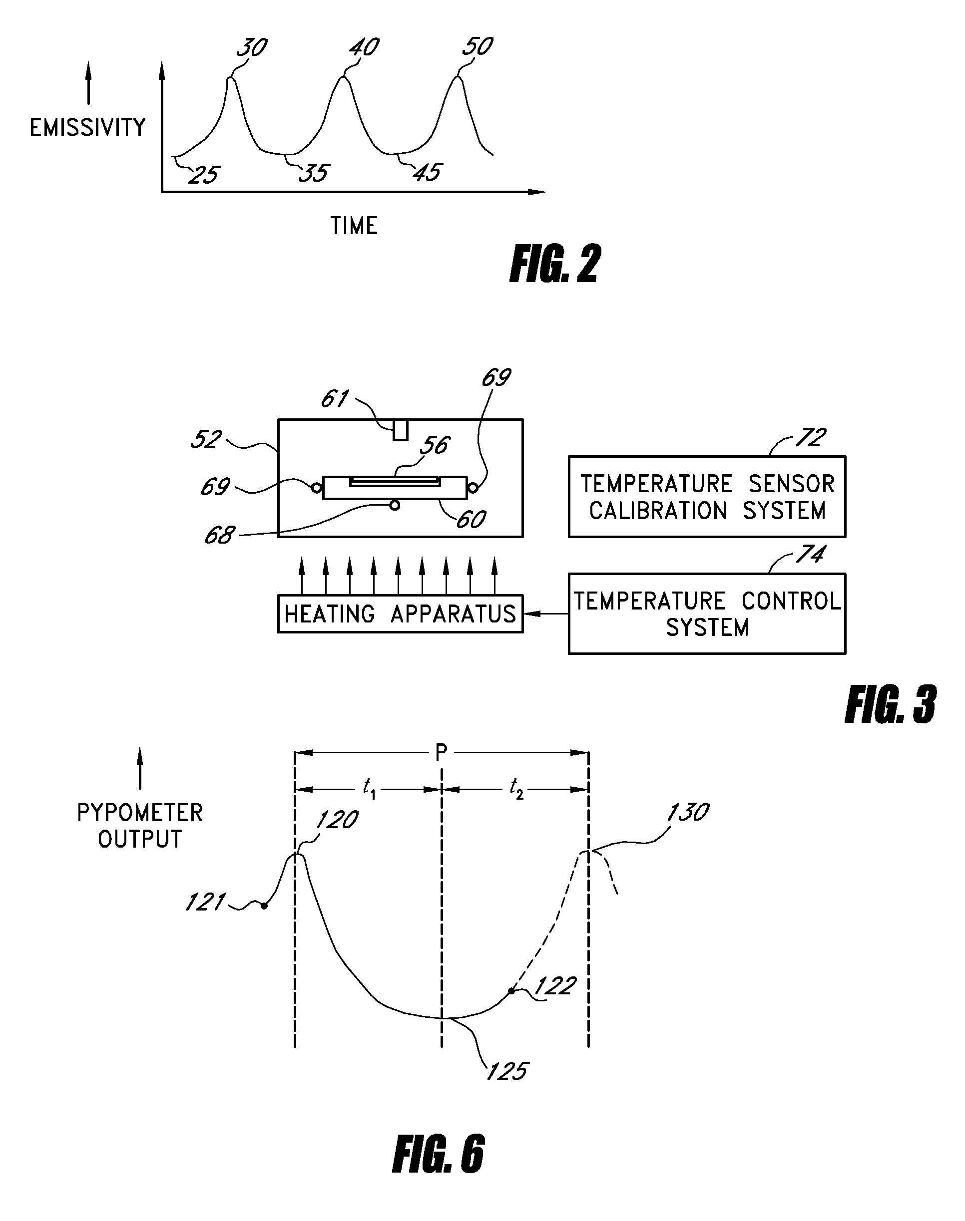
[0014]In one aspect, the present application provides a method of calibrating a temperature control system. In accordance with the method, a heating apparatus, a temperature sensor, and a temperature control system are provided. The heating apparatus is configured to heat a semiconductor processing chamber. The temperature sensor is configured to generate a signal indicative of a temperature within the processing chamber. The temperature control system is configured to control the heating apparatus based on the signal from the temperature sensor. A thickness of a layer of material in the processing chamber is varied. While varying the layer thickness, a variation of a property of the layer is measured, the property having a cyclical variation as a thickness of the layer varies. A cycle time period of the cyclical variation of the property is measured, and the temperature control system is adjusted based on the measured cycle time period.
[0015]In another aspect, the present application provides a method of calibrating a temperature control system. In accordance with the method, a heating apparatus, a temperature sensor, and a temperature control system are provided. The heating apparatus is configured to heat a semiconductor processing chamber. The temperature sensor is configured to generate a signal indicative of a temperature within the processing chamber. The temperature control system is configured to control the heating apparatus based on the signal from the temperature sensor. A thickness of a layer of material in the processing chamber is varied. While varying the layer thickness, a variation of a property of the layer is measured, the property having a cyclical variation as the layer thickness varies. After the measured variation of the property reaches at least one peak and at least one trough, a process duration is determined, the process duration beginning at a first point in the measured variation and ending at a second point in the measured variation. A difference between the process duration and an expected duration is determined, and the temperature control system is adjusted based on the difference.
[0016]In another aspect, the present application provides an apparatus for semiconductor processing. The apparatus comprises a semiconductor processing chamber, a heating apparatus configured to heat the processing chamber, a temperature sensor, a temperature control system, a cyclical property sensor, and a calibration system. The temperature sensor is configured to generate a signal indicative of a temperature within the processing chamber. The temperature control system is configured to control the heating apparatus based on the signal from the temperature sensor. The cyclical property sensor measures a property of a layer of a material in the chamber, the property having a cyclical variation as a thickness of the layer varies. The calibration system is configured to determine a cycle time period of a cyclical variation of the property of a layer of material in the chamber as measured by the cyclical property sensor while a thickness of the layer is varied. The calibration system is also configured to adjust the temperature control system based on the determined cycle time period.
[0017]In yet another aspect, the present application provides an apparatus for semiconductor processing, comprising a semiconductor processing chamber, a heating apparatus configured to heat the processing chamber, a temperature sensor, a temperature control system, a cyclical property sensor, and a calibration system. The temperature sensor is configured to generate a signal indicative of a temperature within the processing chamber. The temperature control system is configured to control the heating apparatus based on the signal from the temperature sensor. The cyclical property sensor measures a property of a layer of a material in the chamber, the property having a cyclical variation as a thickness of the layer varies. The calibration system is configured to determine, after the cyclical property sensor measures a variation of the property of a layer in the chamber and the measured variation reaches at least one peak and at least one trough, a process duration beginning at a first point in the measured variation and ending at a second point in the measured variation. The calibration system is also configured to determine a difference between the process duration and an expected duration, and to adjust the temperature control system based on the determined difference.

Problems solved by technology

Thus, substrate temperature is usually a critical process parameter in the kinetic regime, and a small change in temperature can result in a significant change in deposition rate and an undesirable or non-uniform layer thickness.
However, if direct or reflected light from elements other than the substrate, such as from heating lamps, reaches the pyrometer, then the light radiation emitted from the substrate is only a part of the total radiation that the pyrometer receives, causing inaccuracies in the temperature readings.
One problem in substrate reactors that use thermocouples is thermocouple drift, which is the tendency of thermocouple outputs to shift (i.e., report temperature less accurately, typically with a bias up or down) over time, for example over the course of many runs spanning days, months, or years.
In addition to thermocouple drift, there are a variety of other factors that can lead to inaccuracies in substrate temperature control.
First, if heat lamps are used to heat the wafer, each lamp's power output can vary over time.
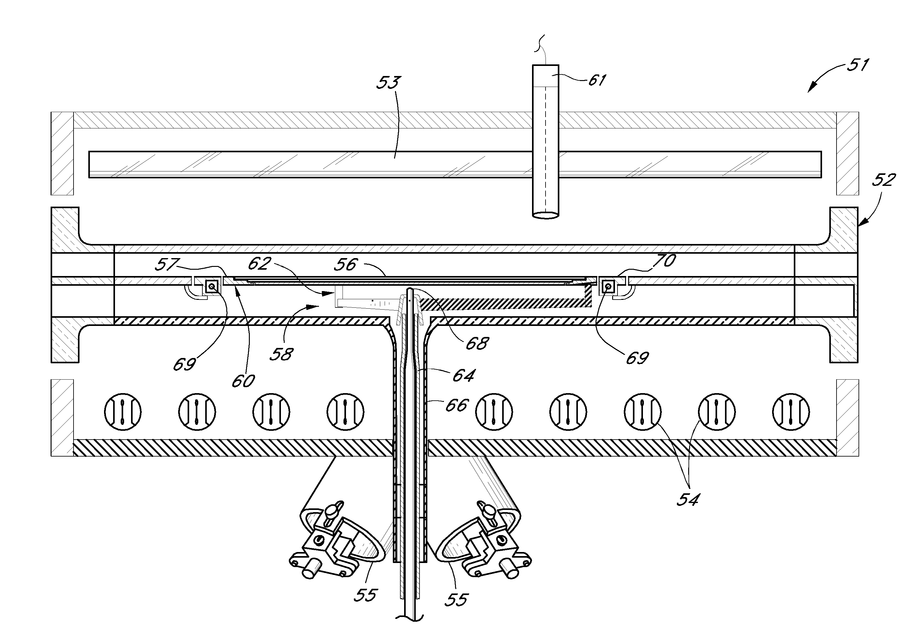
Second, some reactors include reflective surfaces (e.g., gold surfaces) that surround the reaction chamber and reflect radiation toward the substrate and susceptor, and these reflective surfaces can degrade over time.
Third, the emissivity of the susceptor itself can change over time.
Fourth, material deposits (e.g., silicon) on the susceptor (e.g., a graphite susceptor with a silicon carbide coating) can cause temperature shifts as well.
These methods are undesirable in terms of reactor downtime and wafer cost, partly because they involve removing the wafer from the chamber for measuring film thickness or extent of diffusion.
While this method of calibrating a temperature control system is very useful, it is somewhat limited and arbitrary because it depends upon a human technician's visual interpretation of color.

Method used


Image

  • Calibration of temperature control system for semiconductor processing chamber
  • Calibration of temperature control system for semiconductor processing chamber
  • Calibration of temperature control system for semiconductor processing chamber

Examples


Embodiment Construction

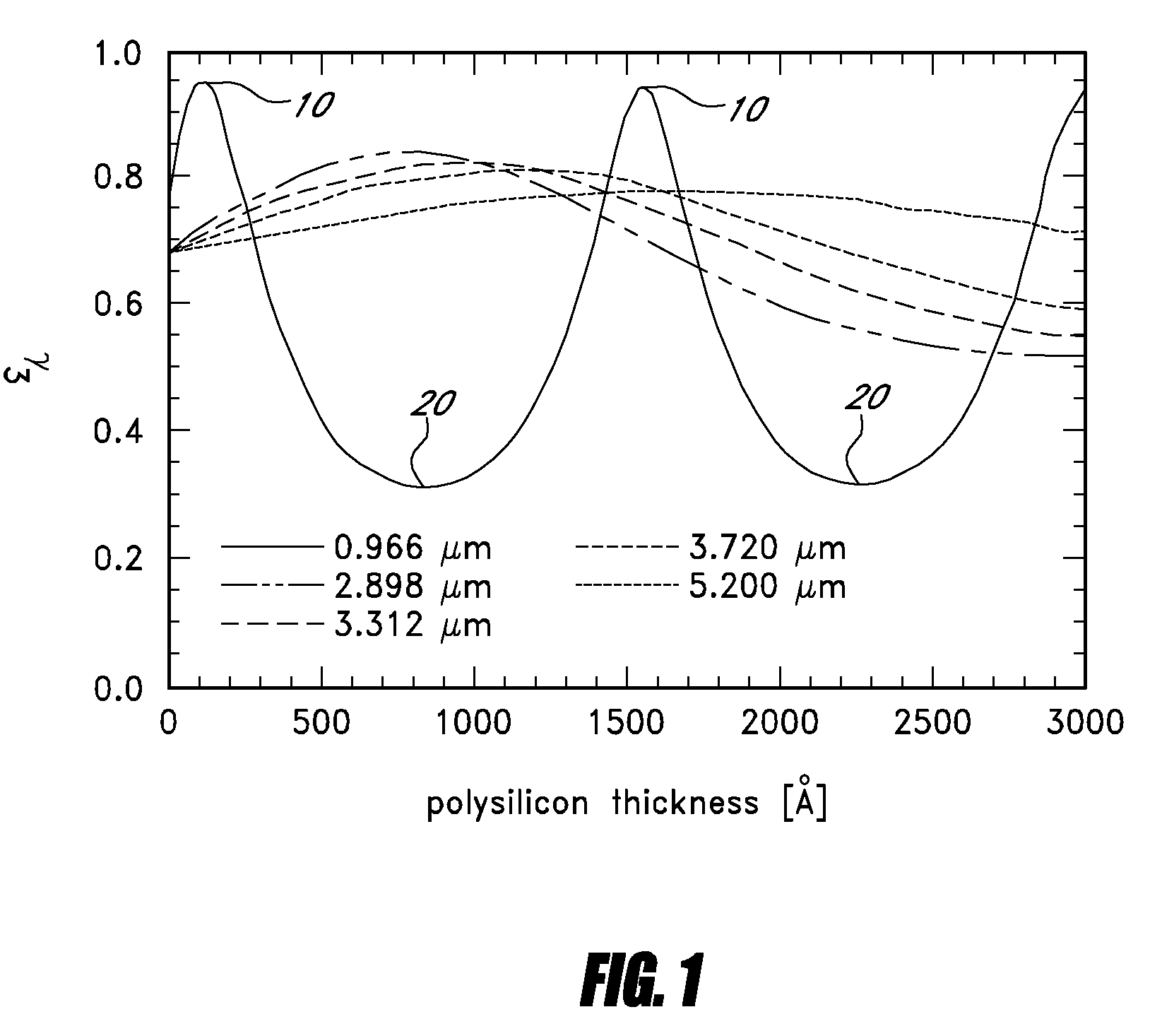
[0029]The present inventors have recognized that, within certain film thickness ranges, certain properties of a deposited film vary cyclically with the film thickness. Such properties are referred to herein as “cyclical properties.” Two such cyclical properties are the film's color and emissivity. For example, the color of a silicon film deposited onto a 1000 Angstrom silicon dioxide layer coating a silicon wafer has been observed to vary as follows:[0030]Blue (this is the base color of the 1000 Angstrom oxide)[0031]Silver (200-300 Angstroms; only seen once as the polysilicon thickens)[0032]Gold (400 Angstroms)[0033]Blue[0034]Green[0035]Gold[0036]Then the above colors repeat (except blue and silver every 500 Angstroms until the layer reaches a certain thickness, such as approximately 4000 Angstroms)

[0037]Similarly, the emissivity of a deposited layer varies cyclically with layer thickness as well. FIG. 1 is a graph showing the emissivity variation as a function of layer thickness at...


PUM


Abstract

Methods and systems for calibrating a temperature control system in a vapor deposition chamber. A temperature sensor senses temperature within a semiconductor processing chamber and generates an output signal. A temperature control system controls a chamber temperature by controlling a heating apparatus based on the output signal. A method includes instructing the control system to target a setpoint temperature, and depositing a layer of material onto a surface in the chamber by a vapor deposition process. A variation of a property of the layer is measured while depositing the layer, the property known to vary cyclically as a thickness of the layer increases. The measured property is allowed to vary cyclically for one or more cycles. If there is a difference between a time period of one or more of the cycles and an expected time period associated with the setpoint temperature, the temperature control system is adjusted based on the difference.

Description

CLAIM FOR PRIORITY[0001]This application claims priority to Provisional Patent Application No. 61 / 012,397, filed on Dec. 7, 2007, the entire disclosure of which is incorporated herein by reference.BACKGROUND OF THE INVENTION[0002]1. Field of the Invention[0003]The present invention relates generally to semiconductor processing equipment and specifically to systems and methods for calibrating a temperature control system for a substrate processing chamber.[0004]2. Description of the Related Art[0005]High temperature processing chambers are used for depositing various material layers onto semiconductor substrates, such as silicon wafers. A substrate is placed on a substrate holder, such as a susceptor, within the processing chamber. Both the substrate and the substrate holder are heated to a desired temperature. In an exemplary substrate treatment step, two or more reactant gases are conveyed over the heated substrate, where they chemically react with one another to cause chemical vap...

Claims


Application Information

Patent Timeline
IPC IPC(8): G01K15/00
CPCG01K15/00
Inventor GOODMAN, MATTHEW G.HAWKINS, MARKAGGARWAL, RAVINDERGIVENS, MICHAELHILL, ERICBARTLETT, GREGORY
Owner ASM IP HLDG BV
Learn More