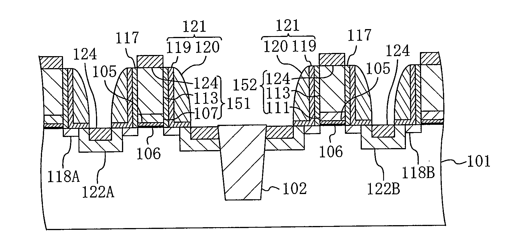
Semiconductor device and method for manufacturing the same
a technology of semiconductors and semiconductors, applied in the direction of semiconductor devices, electrical devices, transistors, etc., can solve the problems of no method established in the art, the capacitance decrease is not easy to detect, and the substrate can be chipped, so as to avoid the risk of lowering the yield and low cost
- Summary
- Abstract
- Description
- Claims
- Application Information
AI Technical Summary
Benefits of technology
Problems solved by technology
Method used
Image

Examples
first embodiment
Third Variation of First Embodiment
[0131]A semiconductor device according to a third variation of the first embodiment of the present invention, and a method for manufacturing the same will now be described with reference to the drawings.
[0132]FIGS. 26A to 26C, 27A to 27C and 28A to 28C are cross-sectional views each showing a step in the method for manufacturing a semiconductor device according to the third variation of the first embodiment of the present invention. In FIGS. 26A to 26C, 27A to 27C and 28A to 28C, like elements to those of the first embodiment shown in FIGS. 1A to 1C, 2A to 2C and 3A to 3C are denoted by like reference numerals and will not be further described below.
[0133]First, a step shown in FIG. 26A is performed, as shown in FIG. 1A of the first embodiment. This variation differs from the first embodiment in that the thickness of the polysilicon film deposited as the first gate electrode material film 107 is about 10 to 40 nm, which is larger, by about a factor...
second embodiment
[0137]A semiconductor device according to a second embodiment of the present invention, and a method for manufacturing the same will now be described with reference to the drawings.
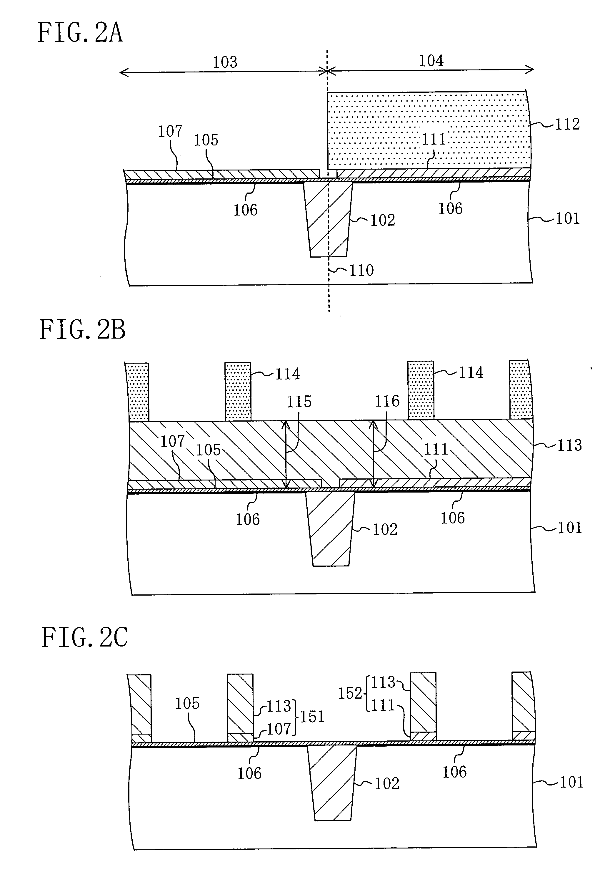
[0138]FIGS. 8A to 8C, 9A to 9C, 10A to 10C and 11A to 11C are cross-sectional views each showing a step in the method for manufacturing a semiconductor device according to the second embodiment of the present invention. In FIGS. 8A to 8C, 9A to 9C, 10A to 10C and 11A to 11C, like elements to those of the first embodiment shown in FIGS. 1A to 1C, 2A to 2C and 3A to 3C are denoted by like reference numerals and will not be further described below.
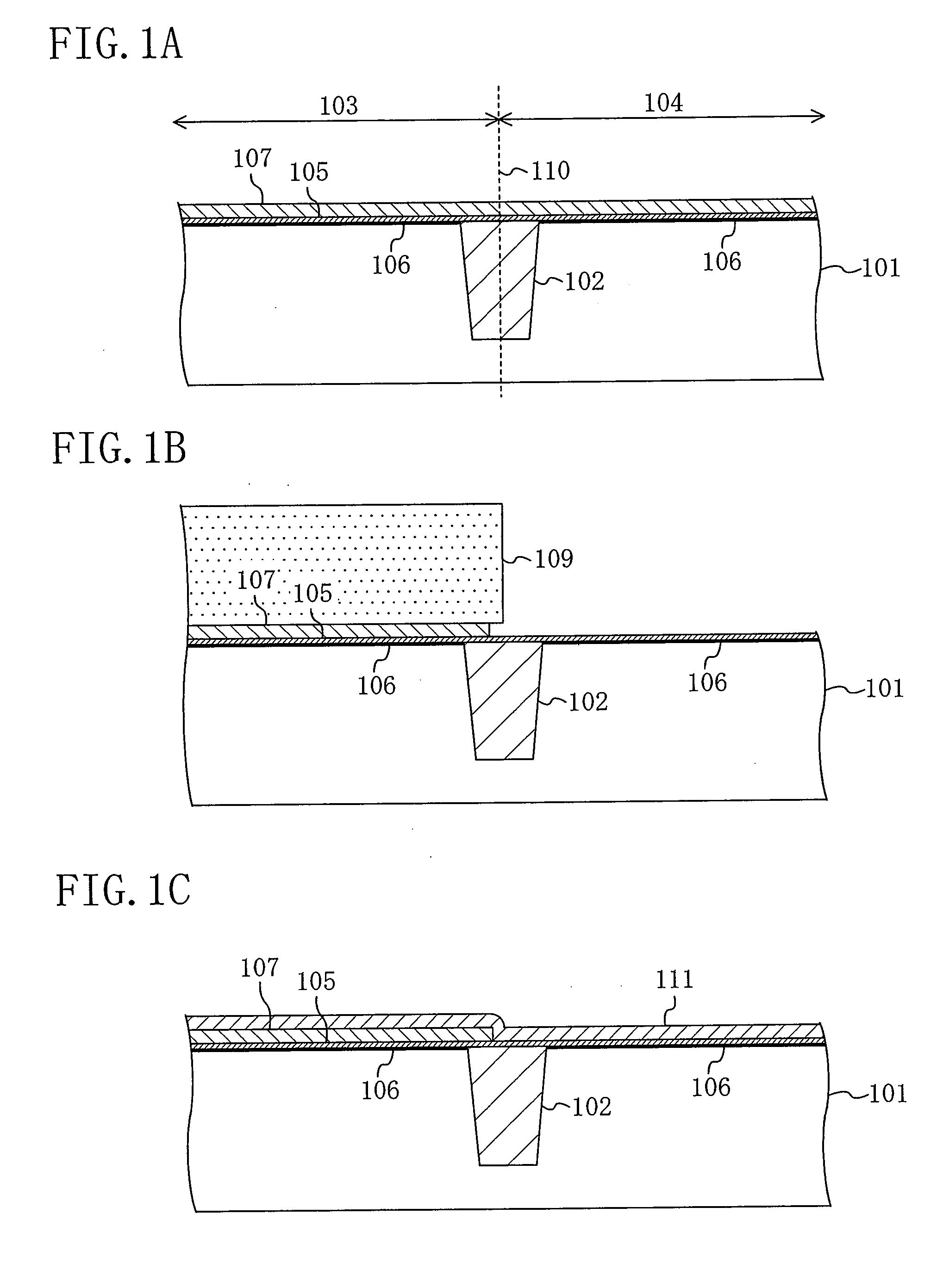
[0139]First, as shown in FIG. 8A, an isolation region 102 such as an STI, for example, is formed in a semiconductor substrate 101 to thereby separate an n-channel region 103 and a p-channel region 104 from each other, after which the n-channel region 103 and the p-channel region 104 are each subjected to a well-forming ion implantation. Then, the n-channel region 1...
third embodiment
[0160]A semiconductor device according to a third embodiment of the present invention, and a method for manufacturing the same will now be described with reference to the drawings.
[0161]FIGS. 12A to 12C, 13A to 13C, 14A to 14C, 15A to 15C and 16A and 16B are cross-sectional views each showing a step in the method for manufacturing a semiconductor device according to the second embodiment of the present invention. In FIGS. 12A to 12C, 13A to 13C, 14A to 14C, 15A to 15C and 16A and 16B, like elements to those of the first embodiment shown in FIGS. 1A to 1C, 2A to 2C and 3A to 3C are denoted by like reference numerals and will not be further described below.
[0162]First, as shown in FIG. 12A, an isolation region 102 such as an STI, for example, is formed in a semiconductor substrate 101 to thereby separate an n-channel region 103 and a p-channel region 104 from each other, after which the n-channel region 103 and the p-channel region 104 are each subjected to a well-forming ion implanta...
PUM
 Abstract
Description
Claims
Application Information
 - R&D
- Intellectual Property
- Life Sciences
- Materials
- Tech Scout
- Unparalleled Data Quality
- Higher Quality Content
- 60% Fewer Hallucinations
Browse by: Latest US Patents, China's latest patents, Technical Efficacy Thesaurus, Application Domain, Technology Topic, Popular Technical Reports.
© 2025 PatSnap. All rights reserved.Legal|Privacy policy|Modern Slavery Act Transparency Statement|Sitemap|About US| Contact US: help@patsnap.com