Crystal Resonator
a crystal resonator and high-frequency technology, applied in piezoelectric/electrostrictive/magnetostrictive devices, piezoelectric/electrostriction/magnetostriction machines, electrical equipment, etc., can solve the problem of frequency jump phenomenon, unstable oscillation, and deterioration of crystal resonator characteristics
- Summary
- Abstract
- Description
- Claims
- Application Information
AI Technical Summary
Benefits of technology
Problems solved by technology
Method used
Image
Examples
first embodiment
[0092]Hereinafter, the present invention will be described with reference to the accompanying drawings. In this embodiment, an AT-cut crystal plate that is driven by a thickness-shear mode will be described. Note that the above-described demonstration experiments on the cut-outs were conducted using the AT-cut crystal plate of the embodiment described below.
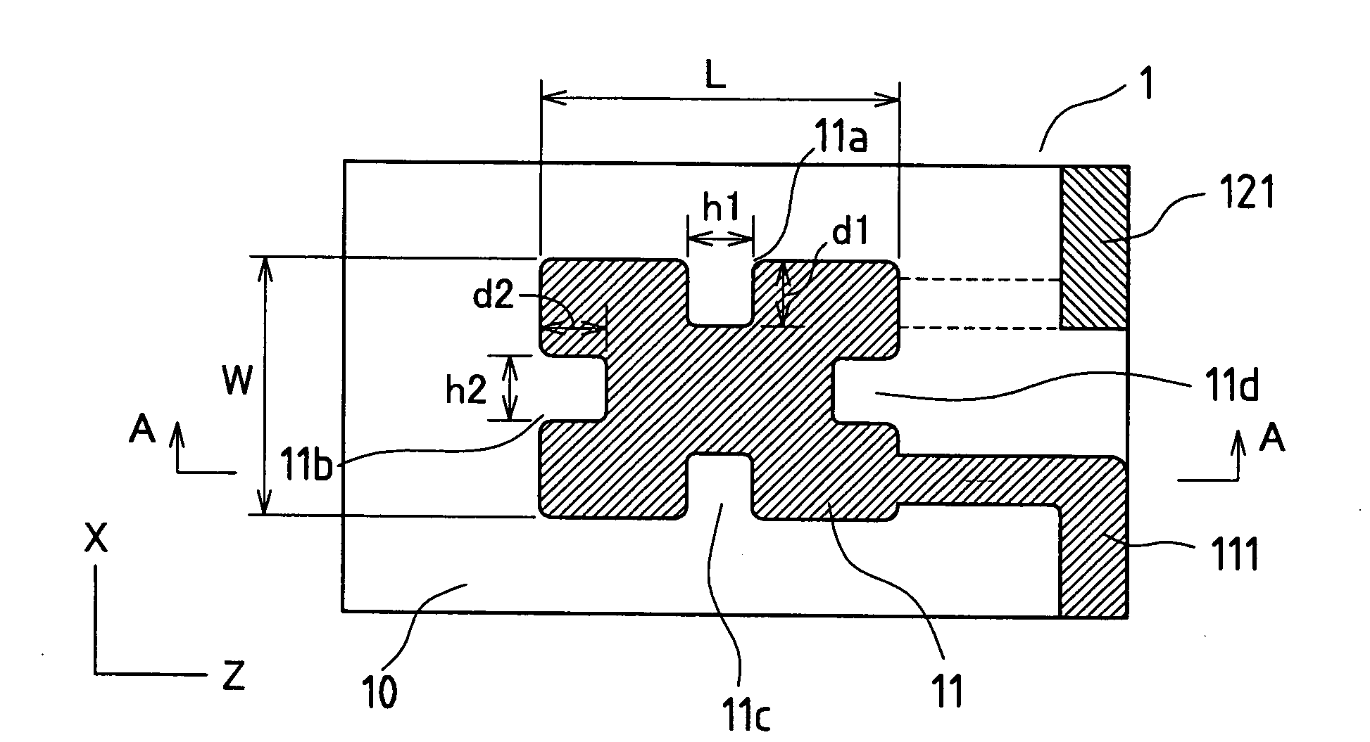
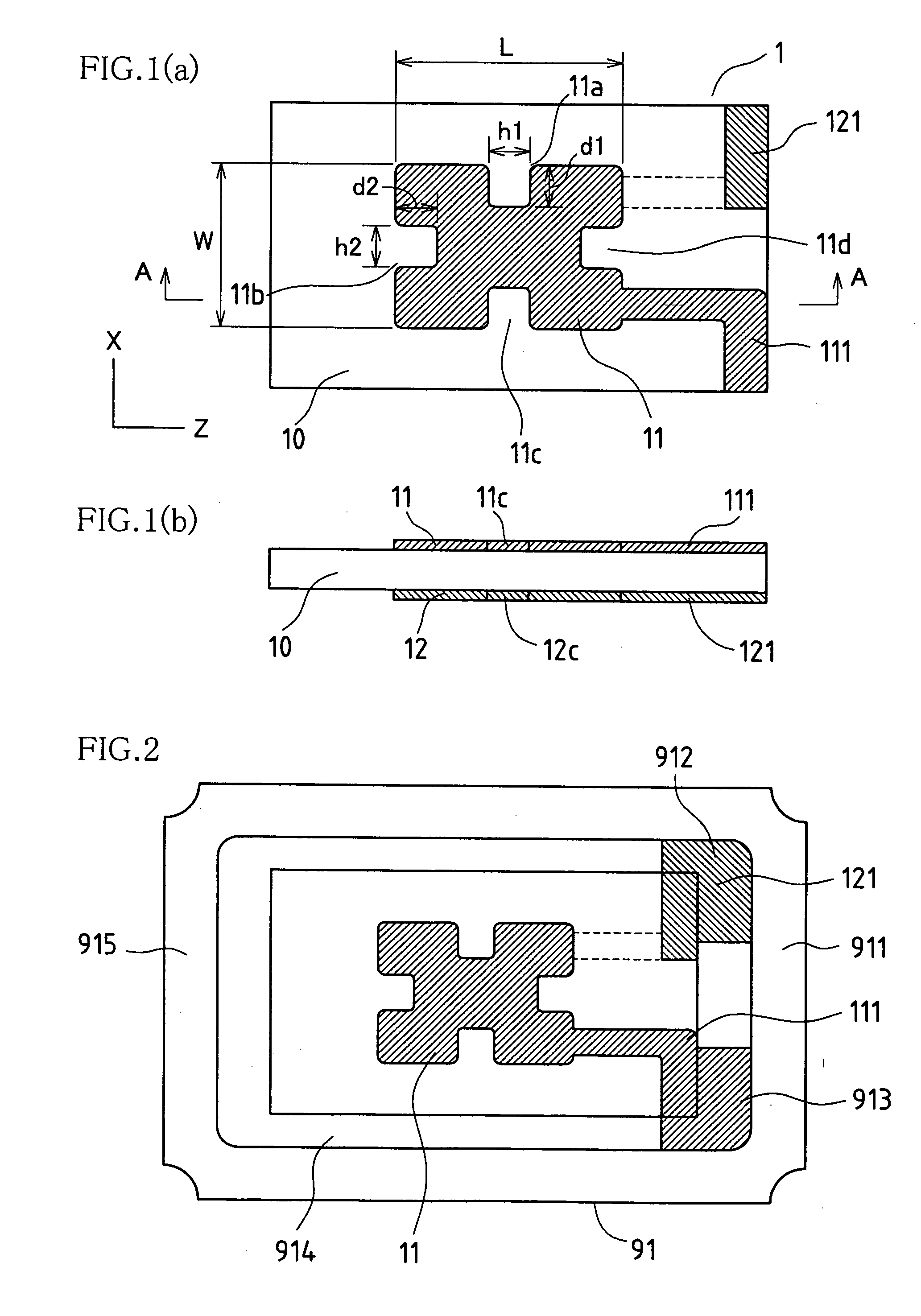
[0093]FIG. 1 is a diagram showing a surface mount crystal resonator. FIG. 1(a) is a plan view of a crystal vibrating element on the front and rear (front and rear surfaces) of which excitation electrodes are formed. FIG. 1(b) is a side view of FIG. 1(a). FIG. 2 is a plan view showing a state in which the crystal vibrating element is housed in a package.
[0094]The crystal vibrating element 1 (hereinafter referred to as a crystal plate) comprises an AT-cut crystal vibrating element in the shape of a plate (a rectangle as viewed from the top). Excitation electrodes 11 and 12 in the shape of a rectangle as viewed from the top are form...
second embodiment
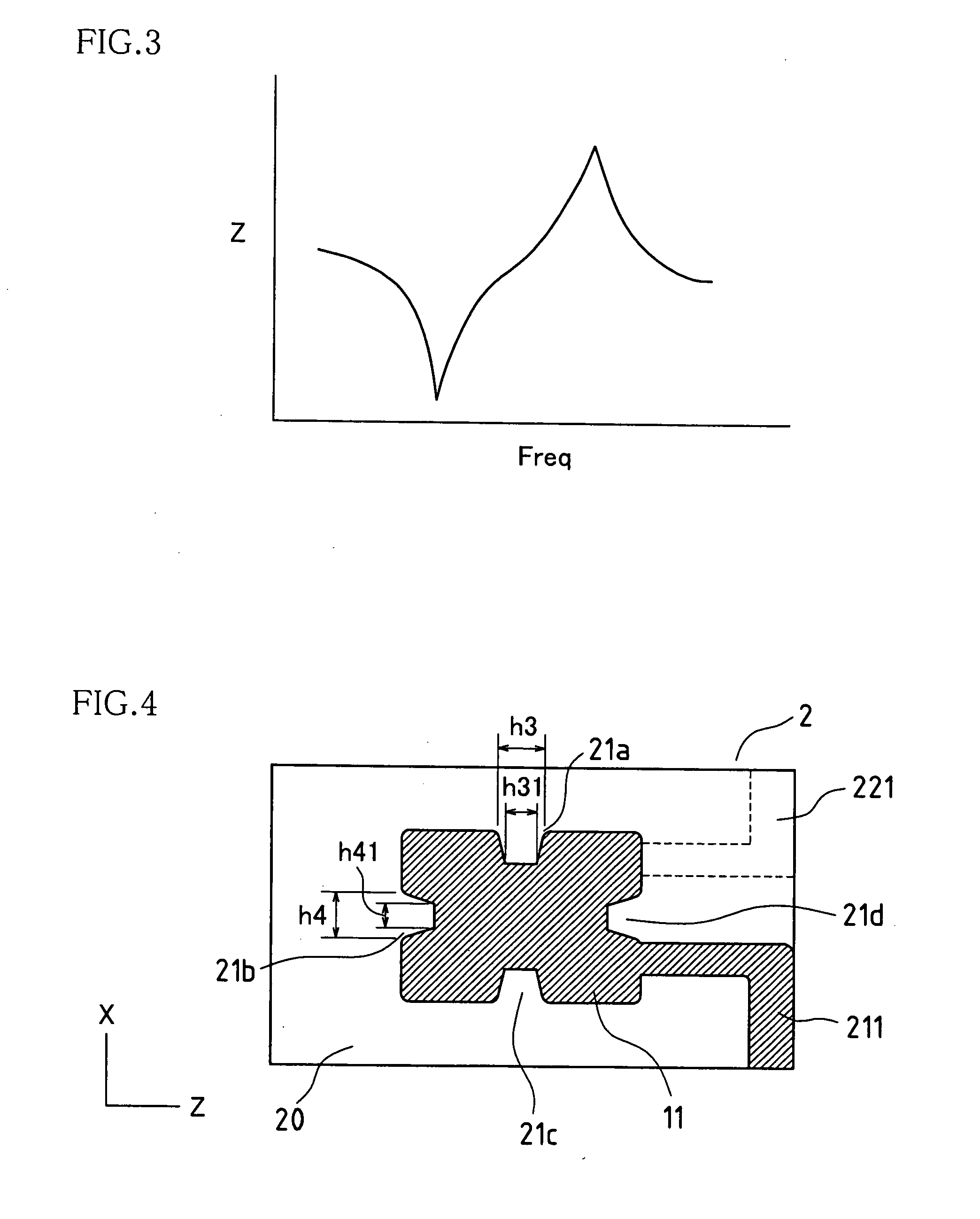
[0099]the present invention will be described with reference to FIG. 4. Also in this embodiment, as is similar to the embodiment above, a crystal vibrating element 2 (hereinafter referred to as a crystal plate) comprises an AT-cut crystal vibrating element in the shape of a plate (a rectangle as viewed from the top). Excitation electrodes 21 and 22 in the shape of a rectangle as viewed from the top are formed in middle regions of the front and rear (front and rear surfaces) of the crystal plate 2. In this embodiment, in the crystal plate 2, the X axis is set to be along the longer sides, and the Z axis is set to be along the shorter sides. Also, the excitation electrodes 21 and 22 have the longer sides along the X axis and the shorter sides along the Z axis.
[0100]Also, the excitation electrodes 21 and 22 have the same shape. Notches 21a, 21b, 21c, 21d, 22a, 22b, 22c and 22d are formed in the excitation electrodes 21 and 22. Note that the excitation electrode 22 formed on the rear su...
third embodiment
[0102]the present invention will be described with reference to FIG. 5. Also in this embodiment, as is similar to the embodiments above, a crystal vibrating element 3 (hereinafter referred to as a crystal plate) comprises an AT-cut crystal vibrating element in the shape of a plate (a rectangle as viewed from the top). Excitation electrodes31 and 32 in the shape of a rectangle as viewed from the top are formed in middle regions of the front and rear (front and rear surfaces) of the crystal plate 3. In this embodiment, in the crystal plate 3, the X axis is set to be along the longer sides, and the Z axis is set to be along the shorter sides. Also, the excitation electrodes 31 and 32 have the longer sides along the X axis and the shorter sides along the Z axis. Also, the excitation electrodes 31 and 32 have the same shape and are exactly opposed to each other via the crystal plate 3. Notches 31a, 31b, 31c, 31d, 32a, 32b, 32c and 32d are formed in middle portions of the sides of the exc...
PUM
 Abstract
Description
Claims
Application Information
 - R&D
- Intellectual Property
- Life Sciences
- Materials
- Tech Scout
- Unparalleled Data Quality
- Higher Quality Content
- 60% Fewer Hallucinations
Browse by: Latest US Patents, China's latest patents, Technical Efficacy Thesaurus, Application Domain, Technology Topic, Popular Technical Reports.
© 2025 PatSnap. All rights reserved.Legal|Privacy policy|Modern Slavery Act Transparency Statement|Sitemap|About US| Contact US: help@patsnap.com


