Method of reducing memory card edge roughness by edge coating

a memory card and edge coating technology, applied in the direction of semiconductor devices, electrical equipment, semiconductor/solid-state device details, etc., can solve the problems of reducing the ejection force of smaller packages from the host device, requiring special cutting methods, and increasing the delicate structure of the host device for receiving and ejecting portable memory packages

Inactive Publication Date: 2009-04-02
SANDISK TECH LLC
View PDF9 Cites 19 Cited by
  • Summary
  • Abstract
  • Description
  • Claims
  • Application Information

AI Technical Summary

Benefits of technology

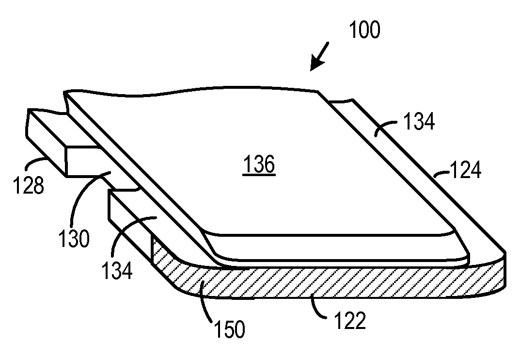
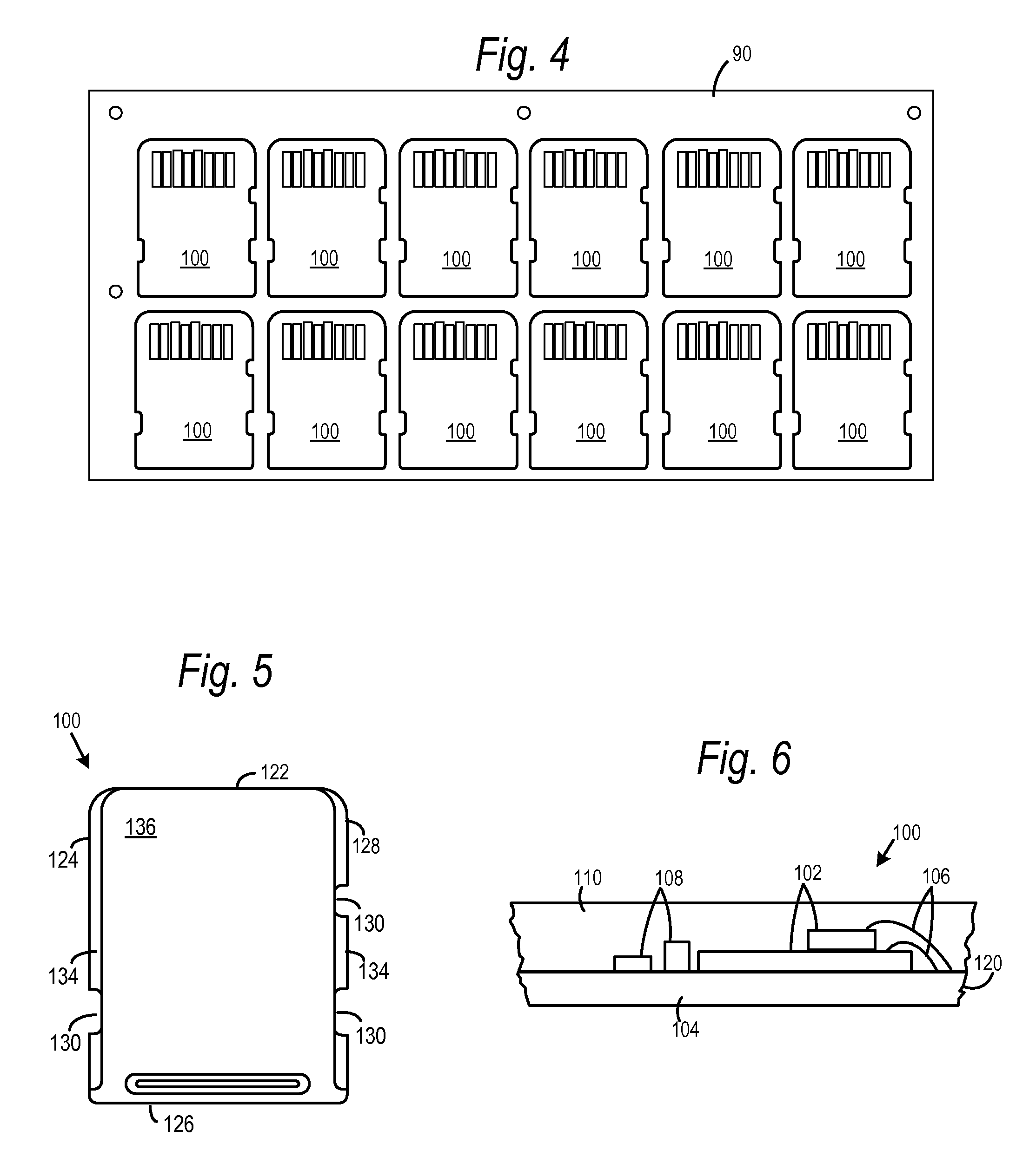
[0012]The present invention, roughly described, relates to a method of forming a semiconductor package with smooth edges, and a semiconductor package formed thereby. In embodiments, after encapsulation, the semiconductor package may be at least partially singulated from the panel by making one or more cuts through the panel to define one or more edges of the semiconductor package. According to embodiments of the invention, the one or more edges may be smoothed by applying a laminate to the edges. The edges receiving the laminate may include any edge between a top and bottom surface of the package.

Problems solved by technology

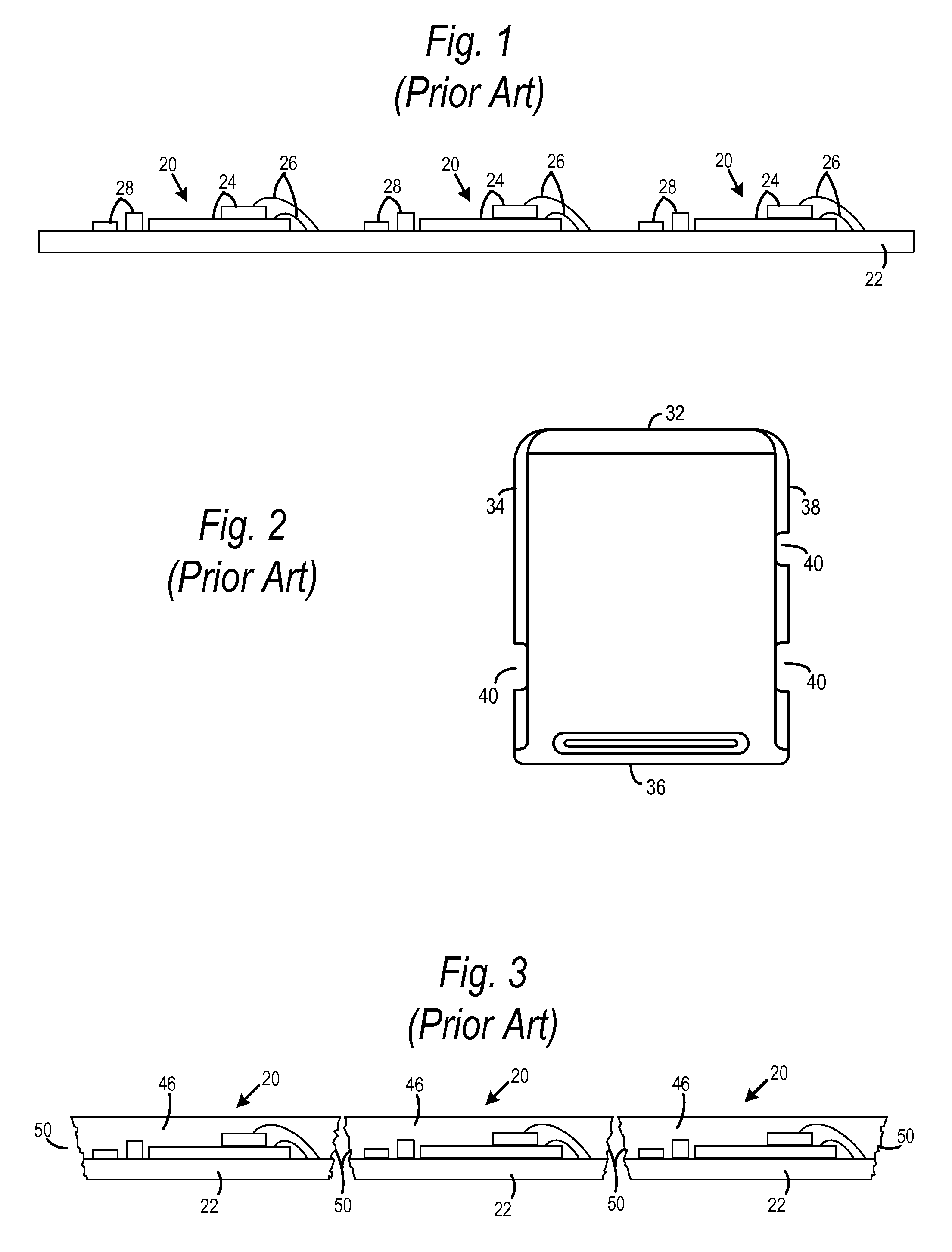
However, specialized cutting methods are required for cutting curvilinear shaped edges during singulation.
As semiconductor packages continue to shrink, the structure within a host device for receiving and ejecting portable memory packages is becoming more delicate, and the ejection force with which smaller packages are ejected from the host device is getting smaller.
Consequently, the roughness of the edges of portable memory packages is becoming a significant factor in package design, as small memory cards having rough edges may get stuck inside the host device.
However, such methods do not sufficiently reduce edge roughness, and the tooling and equipment required adds cost to the fabrication process.

Method used


Image

  • Method of reducing memory card edge roughness by edge coating
  • Method of reducing memory card edge roughness by edge coating
  • Method of reducing memory card edge roughness by edge coating

Examples


Embodiment Construction

[0024]The embodiments of the present invention will now be described with reference to FIGS. 4 through 9, which generally relate to a method of forming a semiconductor package including a laminate for reducing the surface roughness of package edges, and a semiconductor package formed thereby. It is understood that the present invention may be embodied in many different forms and should not be construed to being limited to the embodiments set forth herein. Rather, these embodiments are provided so that this disclosure will be thorough and complete and will fully convey embodiments of the invention to those skilled in the art. Indeed, the invention is intended to cover alternatives, modifications and equivalents of these embodiments, which are included within the scope and spirit of the invention as defined by the appended claims. Furthermore, in the following detailed description of embodiments of the present invention, numerous specific details are set forth in order to provide a th...


PUM


Abstract

A method of forming a semiconductor package with smooth edges, and a semiconductor package formed thereby is disclosed. In embodiments, after encapsulation, the semiconductor packages may be at least partially singulated from the panel by making one or more cuts through the panel to define one or more edges of the semiconductor package. The one or more edges may be smoothed by applying a laminate to the edges. The edges receiving the laminate may include any edge between a top and bottom surface of the package.

Description

BACKGROUND OF THE INVENTION[0001]1. Field of the Invention[0002]Embodiments of the present invention relate to methods of smoothing the edges of a portable memory card and a memory card formed thereby.[0003]2. Description of the Related Art[0004]As the sizes of electronic devices continue to decrease, the associated semiconductor packages that operate within them are being designed with smaller form factors, lower power requirements and higher functionality. Currently, sub-micron features in semiconductor fabrication are placing higher demands on package technology including higher lead counts, reduced lead pitch, minimum footprint area and significant overall volume reduction.[0005]While a wide variety of packaging configurations are known, flash memory storage cards may in general be fabricated as system-in-a-package (SiP) or multichip modules (MCM), where a plurality of die are mounted on a substrate. The substrate may in general be a printed circuit board, a leadframe or a tape ...

Claims


Application Information

Patent Timeline
Patent Type & Authority Applications(United States)
IPC IPC(8): H01L23/29H01L21/00
CPCH01L21/56H01L2924/01033H01L23/3121H01L24/97H01L2224/48091H01L2224/48227H01L2224/97H01L2924/01029H01L2924/01046H01L2924/01047H01L2924/01079H01L2924/01082H01L2924/01088H01L2924/1433H01L2924/19041H01L21/561H01L2924/01006H01L2924/01005H01L24/48H01L2224/85H01L2924/00014H01L2924/14H01L2924/181
Inventor HOO, ONG KINGZHU, JAVAYE, NINGTAKIAR, HEM
Owner SANDISK TECH LLC
Why Eureka
Try Eureka