
Test Method and Test Program of Semiconductor Logic Circuit Device

a test method and logic circuit technology, applied in the direction of detecting faulty computer hardware, error detection/correction, instruments, etc., can solve the problems of power consumption remarkably larger in the test mode than in the usual operation mode, and the controllability of the pseudo external input line and the observability of the pseudo external output line. , to achieve the effect of reducing the power supply voltage, avoiding an error-prone test, and reducing the power consumption

Inactive Publication Date: 2009-03-26
WEN XIAOQUING +1
View PDF13 Cites 9 Cited by
  • Summary
  • Abstract
  • Description
  • Claims
  • Application Information

AI Technical Summary

Benefits of technology

[0029]According to the present invention, since the number of output switching scan flip-flops in a capture operation is decreased, the capture power consumption can be decreased, thus avoiding an erroneous test caused by the decrease of the power supply voltage due to the IR drop.

Problems solved by technology

However, it is generally impossible to directly access the output lines of the flip-flops (the pseudo external input lines) and the input lines of the flip-flops (the pseudo external output lines) in the semiconductor logic circuit device from the exterior.
Therefore, in order to test the combinational portion, there are problems in the controllability of the pseudo external input lines and the observableness of the pseudo external output lines.
Despite the effectiveness of the above-mentioned scan test method, there is a problem in that the power consumption is remarkably larger in a test mode than in a usual operation mode.
For example, if the semiconductor logic circuit device is constructed by CMOS circuits, the power consumption consists of static power consumption due to leakage currents and dynamic power consumption due to switching operations of the logic gates and the flip-flops.
Additionally, the latter dynamic power consumption consists of shift power consumption in shift operations and capture power consumption in capture operations.
As a result, the shift power consumption is increased to induce excessive heat.
Therefore, semiconductor logic circuit devices would be damaged.
Thus, even semiconductor logic circuit devices normally operable in a usual state would be deemed to be defective in a test state, which can be an erroneous test.
As a result, the manufacturing yield would be decreased.
Particularly, when semiconductor logic circuit devices become ultra-large in scale, more fine-structured and lower in power supply voltage, the manufacturing yield caused by the erroneous test would be remarkably decreased.
Also, when multiple clock signals are used in a test mode, the capture power consumption can be decreased by a one hot technique or a multiple clock technique; however, the former technique would remarkably increase test data amount, and the latter technique would require enormous memory consumption in generating test vectors which is a large burden to an ATPG.

Method used


Image

  • Test Method and Test Program of Semiconductor Logic Circuit Device
  • Test Method and Test Program of Semiconductor Logic Circuit Device
  • Test Method and Test Program of Semiconductor Logic Circuit Device

Examples


Embodiment Construction

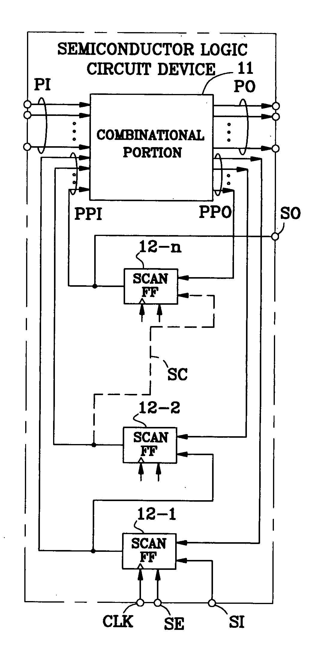
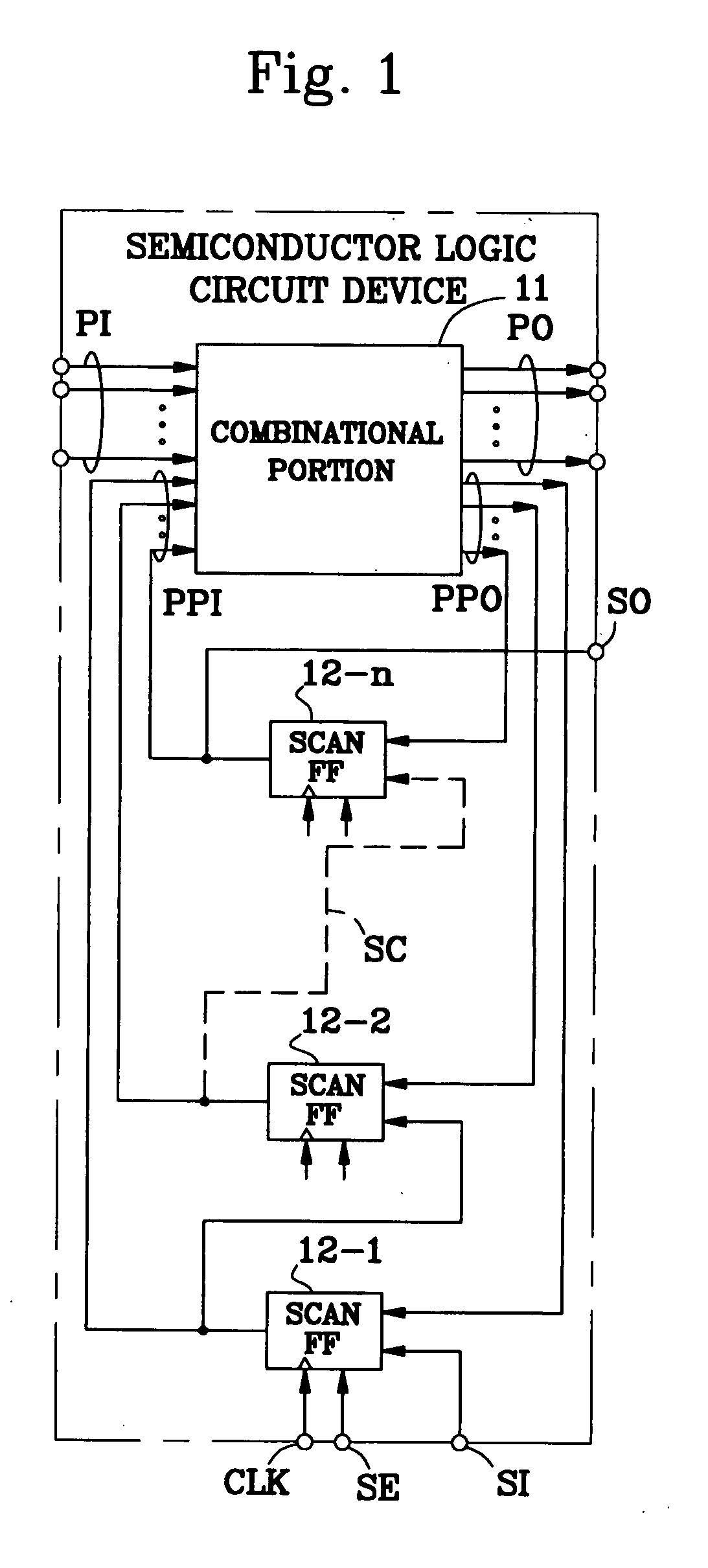
[0045]FIG. 1 is a block circuit diagram illustrating an embodiment of the semiconductor logic circuit device according to the present invention.

[0046]The semiconductor logic circuit device of FIG. 1 is constructed by a combinational portion 11 formed by logic elements such as AND (AND) gates, OR (OR) gates, NAND (NAND) gates, and NOR (NOR) gates, and scan flip-flops 12-1, 12-2, . . . , 12-n.

[0047]The combinational portion 11 has external input lines PI, pseudo external input lines PPI serving as output lines of the scan flip-flops 12-1, 12-2, . . . , 12-n, external output lines PO, and pseudo external output lines PPO serving as input lines of the scan flip-flops 12-1, 12-2, . . . , 12-n. Note that the number of the external input lines PI is not always the same as that of the external output lines PO; however, the number of the pseudo external input lines PPI is always the same as that of the pseudo external output lines PPO.

[0048]In each of the scan flip-flops 12-1, 12-2, . . . , ...


PUM


Abstract

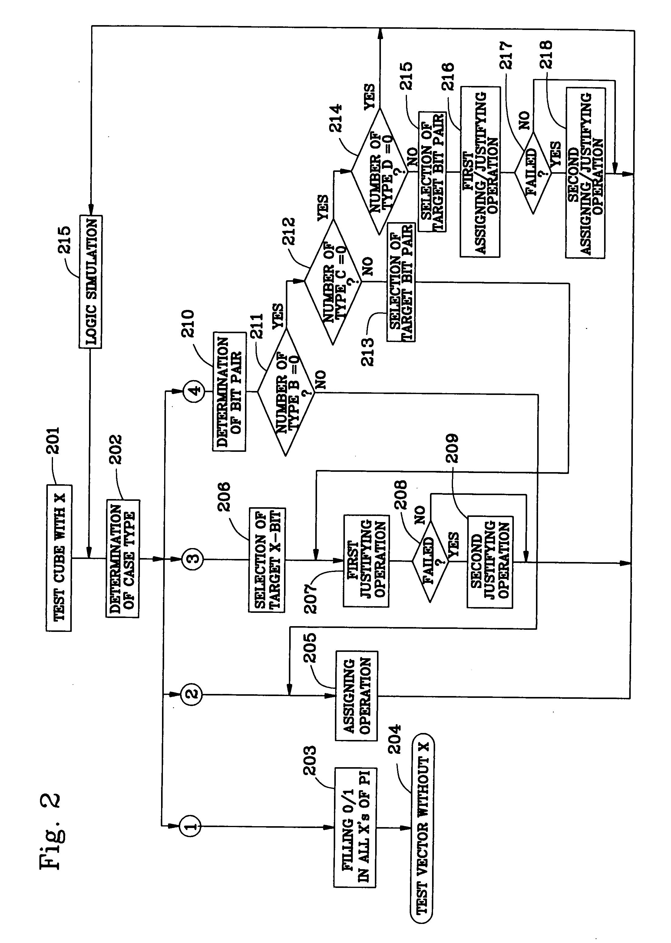
The number of output switching scan flip-flops in a capture operation is decreased, which decreases the capture power consumption, so that the reduction of the power supply voltage can be decreased to decrease generation of an erroneous test. For this purpose, 0 or 1 is filled in unspecified bits within a test cube to decrease the output switching scan flip-flops, to convert the test cube into a test vector with no unspecified bit X. In a combinational portion 11, when there is one or more unspecified bits X in pseudo external input lines PPI and there is no unspecified bit X in pseudo external output lines PPO, an assigning operation is carried out so that the same logic values as bits of the pseudo external output lines PPO corresponding to all the unspecified bits X are assigned thereto (step 205). In the combinational portion 11, when there is one or more unspecified bits X in the pseudo external output lines PPO and there is no unspecified bit X in the pseudo external input lines PPI, first and second justifying operations are carried out, i.e., one unspecified bit X of the pseudo external output lines PPO is selected as a target unspecified bit X, and a necessary logic value is determined for an unspecified bit X of the test cube so that the same logic value as a bit of the pseudo external input lines PPI corresponding to that unspecified bit X or its opposite logic value may appear at that unspecified bit X (steps 207 and 209). In the combinational portion, when there are one more unspecified bits not only in the pseudo external input lines PPI but also the pseudo external output lines PPO, an assigning operation, a justifying operation or first and second assigning / justifying operations are performed upon a focused bit pair “ppi” and “ppo” (steps 210 to 218).

Description

TECHNICAL FIELD[0001]The present invention relates to a test method and test program of a semiconductor logic circuit device.BACKGROUND TECHNOLOGY[0002]Semiconductor logic circuit devices are shipped through three steps, i.e., a design step, a production step and a test step. Here, a test is to apply a test vector upon a manufactured semiconductor logic circuit device, to observe a test response from the semiconductor logic circuit device, and to compare the test response with an expected test response, thus determining whether the semiconductor logic circuit device is good or defective. The rate of good semiconductor logic circuit devices is called a manufacturing yield which would remarkably affect the semiconductor logic circuit devices in quality, reliability and manufacturing cost.[0003]Generally, a semiconductor logic circuit device (mainly, a sequential circuit) is constructed by a combinational portion formed by logic elements such as AND (AND) gates, NAND (NAND) gates, OR (...

Claims


Application Information

Patent Timeline
IPC IPC(8): G01R31/3177G06F11/25
CPCG01R31/318547G01R31/318502
Inventor WEN, XIAOQINGKAJIHARA, SEIJI
Owner WEN XIAOQUING
Learn More