
Method for forming catalyst nanoparticles for growing elongated nanostructures

a nanoparticle and nanostructure technology, applied in physical/chemical process catalysts, metal/metal-oxide/metal-hydroxide catalysts, instruments, etc., can solve the problems of inability to fully realize similar applications, inability to synthesise large-scale, and inability to meet the requirements of the application

Inactive Publication Date: 2009-03-19
INTERUNIVERSITAIR MICRO ELECTRONICS CENT (IMEC VZW)
View PDF1 Cites 57 Cited by
  • Summary
  • Abstract
  • Description
  • Claims
  • Application Information

AI Technical Summary

Benefits of technology

[0013]Furthermore, methods according to preferred embodiments can allow the growth of elongated nanostructures such as CNTs with control over the diameter, number, density and length of the elongated nanostructures.
[0014]The methods according to preferred embodiments provide a way for placing catalytic nanoparticles on sidewalls of a three-dimensional structure and hence provide an alternative for state of the art techniques such as sputtering nanoparticles onto the sidewalls of existing three-dimensional structures, which may be difficult for e.g. narrow interconnect structures.
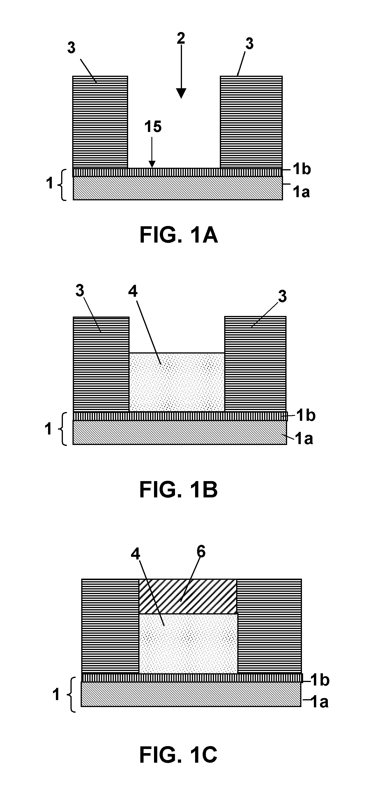
[0035]According to preferred embodiments the method may furthermore comprise providing a capping layer on top of the non-catalytic matrix before selectively removing at least part of the non-catalytic matrix at the sidewalls of the three-dimensional structure. The capping layer may be for preventing elongated nanostructure to be grown on the top of the three-dimensional structures.
[0045]According to preferred embodiments, the method may furthermore comprise providing a capping layer on top of the non-catalytic matrix before selectively removing at least part of the non-catalytic matrix at the sidewalls of the three-dimensional structure. The capping layer may be for preventing elongated nanostructure to be grown on the top of the three-dimensional structures.

Problems solved by technology

These and similar applications cannot be fully accomplished yet since the fabrication of nanostructures still faces a variety of unsolved issues, which vary from one application to another but may, however, be similar in some aspects.
A first issue is related to the growth of nanostructures in a direction substantially parallel to a main surface of a substrate, i.e. in a direction, when the main surface of the substrate is lying in a plane, substantially parallel to the plane of the main substrate.
Hence, this technique is not suitable for, for example, interconnect applications where the connections need to go in all possible directions in a plane substantially parallel to a main surface of a substrate.
However, this synthesis is very localized and restricted by the size of a laser spot used.
Forming more CNTs, or in other words providing a higher density of CNTs on the substrate would be very cost-and time-ineffective because for this purpose the laser spot would have to be moved over the whole surface of the substrate.
This technique is thus not well suited to obtain a high density of CNTs or NWs, e.g. a density of higher than 1012 cm−2, needed for interconnect applications.
The technique is therefore not suitable for being used for mass production of CNTs.
Another issue is that the existing methods of manufacturing the above-mentioned nanostructures are not particularly compatible with standard, existing semiconductor processing techniques.
However, in this approach use is made of silicon towers that are 10 μm high and it is difficult to make the method compatible with or to incorporate it in state of the art semiconductor processing.

Method used


Image

  • Method for forming catalyst nanoparticles for growing elongated nanostructures
  • Method for forming catalyst nanoparticles for growing elongated nanostructures
  • Method for forming catalyst nanoparticles for growing elongated nanostructures

Examples


Embodiment Construction

[0067]The following description and examples illustrate various preferred embodiments. It will be appreciated that there are numerous variations and modifications of these embodiments that are possible. Accordingly, the descriptions of the various embodiments should not be deemed to limit the scope of the invention, which is defined by the claims.

[0068]The terms top, bottom and the like in the description and the claims are used for descriptive purposes and not necessarily for describing relative positions. It is to be understood that the terms so used are interchangeable under appropriate circumstances and that the preferred embodiments described herein are capable of operation in other orientations than described or illustrated herein.

[0069]It is to be noticed that the term “comprising”, used in the claims, should not be interpreted as being restricted to the means listed thereafter; it does not exclude other elements or steps. It is thus to be interpreted as specifying the presen...


PUM

PropertyMeasurementUnit
Temperatureaaaaaaaaaa
Structureaaaaaaaaaa

Abstract

Preferred embodiments provide a method for forming at least one catalyst nanoparticle on at least one sidewall of a three-dimensional structure on a main surface of a substrate, the main surface lying in a plane and the sidewall of the three-dimensional structure lying in a plane substantially perpendicular to the plane of the main surface of the substrate. The method comprises obtaining a three-dimensional structure on the main surface, the three-dimensional structure comprising catalyst nanoparticles embedded in a non-catalytic matrix and selectively removing at least part of the non-catalytic matrix at the sidewalls of the three-dimensional structure to thereby expose at least one catalyst nanoparticle. According to preferred embodiments a method is also provided for forming at least one elongated nanostructure, such as e.g. a nanowire or carbon nanotube, using the catalyst nanoparticles formed by the method according to preferred embodiments as a catalyst. The methods according to preferred embodiments may be used in, for example, semiconductor processing. The methods according to preferred embodiments are scalable and fully compatible with existing semiconductor processing technology.

Description

CROSS-REFERENCE TO RELATED APPLICATIONS[0001]This application claims the benefit under 35 U.S.C. § 119(e) of U.S. Provisional Application No. U.S. 60 / 948,382 filed on Jul. 6, 2007, and claims the benefit under 35 U.S.C. § 119(a)-(d) of European Application No. 07075889.1 filed on Oct. 16, 2007, the disclosures of which are hereby expressly incorporated by reference in their entirety and are hereby expressly made a portion of this application.FIELD OF THE INVENTION[0002]Methods for formation of catalyst nanoparticles are provided. More particularly, a method for providing at least one catalyst nanoparticle on at least one sidewall of a three-dimensional structure is provided. A method for forming at least one elongated nanostructure on at least one sidewall of a three-dimensional structure using such a catalyst nanoparticle as a catalyst is also provided.BACKGROUND OF THE INVENTION[0003]Nanostructures such as Nanowires (NWs) and Carbon Nanotubes (CNTs) have been identified as one of ...

Claims


Application Information

Patent Timeline
IPC IPC(8): H01L29/12G03F7/20C25D5/02H01L21/20
CPCB01J23/75B01J35/0013B01J37/06B82Y10/00B82Y30/00B82Y40/00H01L2221/1094C01B31/0293H01L21/76876H01L21/76879H01L51/0002H01L51/0048C01B31/0233C01B32/162C01B32/18H10K71/10H10K85/221B01J35/23
Inventor RADISIC, ALEKSANDARVEREECKEN, PHILIPPE M.
Owner INTERUNIVERSITAIR MICRO ELECTRONICS CENT (IMEC VZW)
Learn More