
Method and apparatus for modeling a vectorial polarization effect in an optical lithography system

a vectorial polarization and optical lithography technology, applied in the field of semiconductor manufacturing, can solve the problems of inability to find exact formulae to predict, limited effect of corrected mask patterns, and inability to accurately model the polarization behavior of optical lithography systems, etc., to achieve accurate modeling of polarization effects and enhance lithography models.

Inactive Publication Date: 2009-03-12
SYNOPSYS INC
View PDF4 Cites 21 Cited by
  • Summary
  • Abstract
  • Description
  • Claims
  • Application Information

AI Technical Summary

Benefits of technology

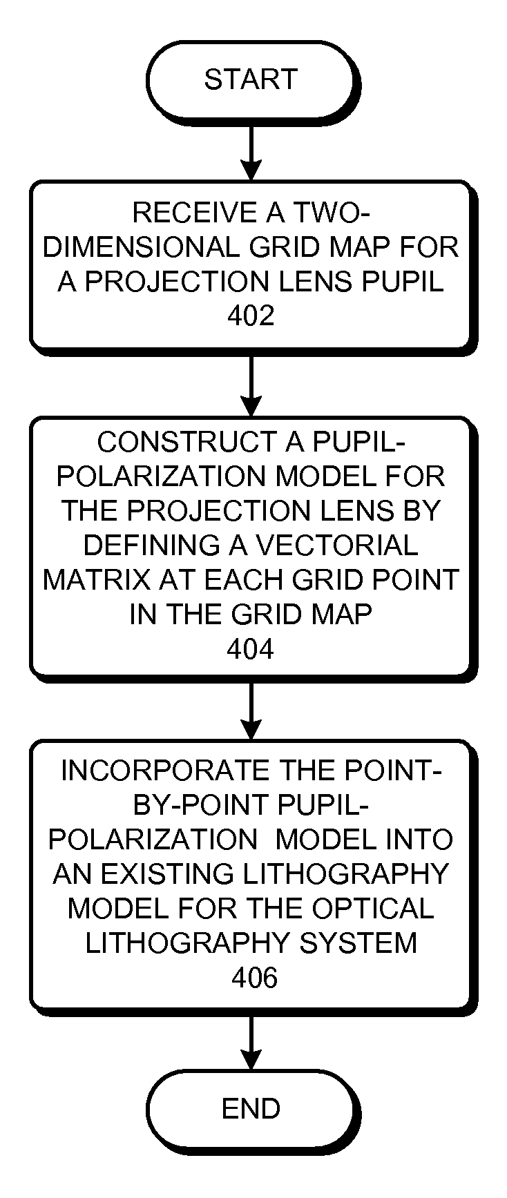
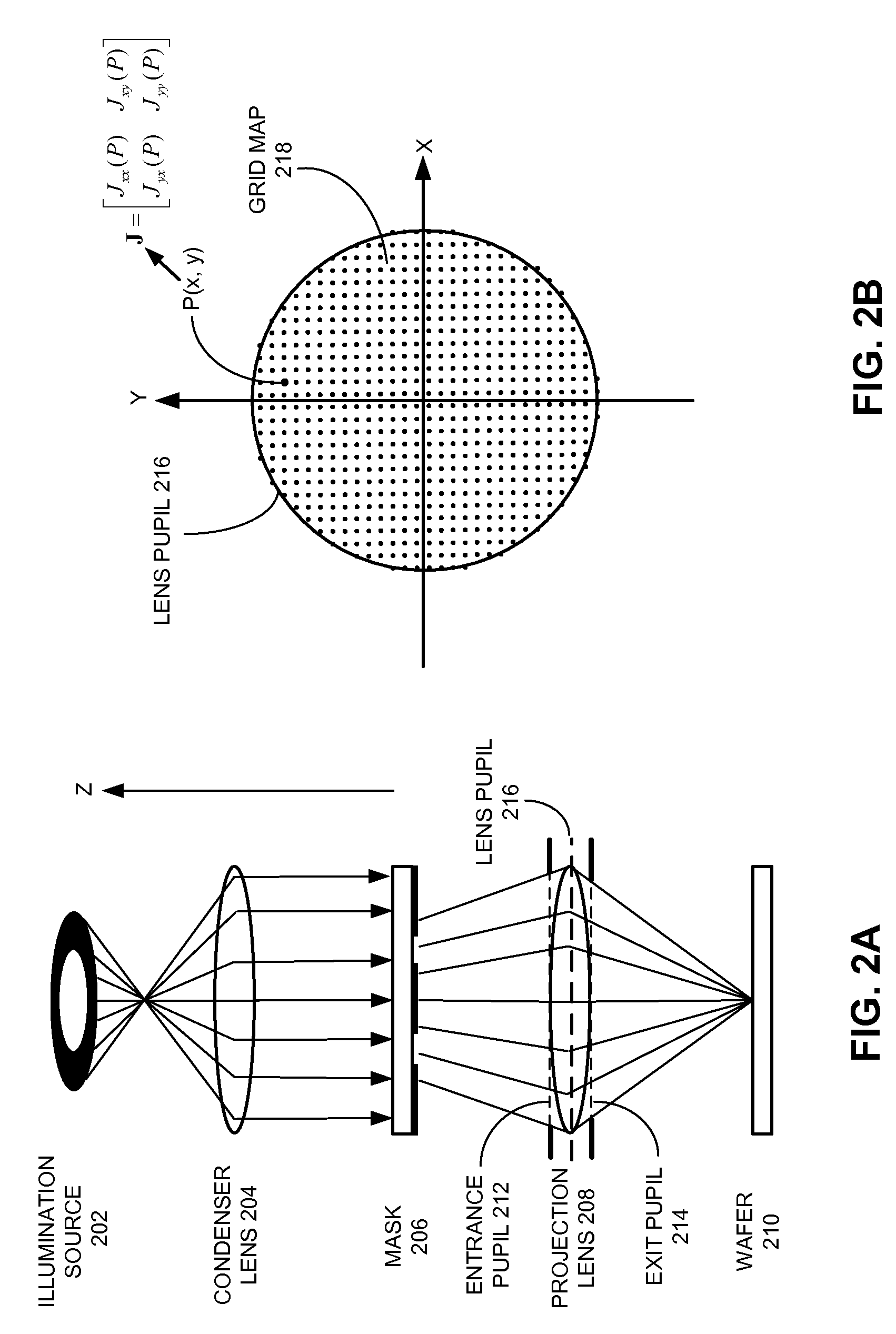
[0011]One embodiment of the present invention provides a system that accurately models polarization effects in an optical lithography system for manufacturing integrated circuits. During operation, the system starts by receiving a polarization-description grid map for a lens pupil in the optical lithography system. The system then constructs a pupil-polarization model by defining a vectorial matrix at each grid point in the grid map, wherein the vectorial matrix specifies a pupil-induced polarization effect on an incoming optical field at the grid point. Next, the system enhances a lithography model for the optical lithography system by incorporating the pupil-polarization model into the lithography / OPC model. The system then uses the enhanced lithography model to perform convolutions with circuit patterns on a mask in order to simulate optical lithography pattern printing.

Problems solved by technology

Since it is almost impossible to find exact formulae to predict the behavior of these complex interactions, developers typically use process models which are fit to empirical data to predict the behavior of these processes.
Note that the effectiveness of the corrected mask patterns is typically limited by the accuracy of the OPC model.
In particular, the polarization behavior of an optical lithographic system is one of the physical effects that are inadequately represented in a traditional OPC model.
While existing OPC models can model the polarization behavior of light and optical lithographic systems in some very limited aspects (i.e., polarization-state-dependent refraction, transmission and reflection in thin films on a wafer), these models are not capable of modeling the more complex polarization-state-dependent vectorial behavior of light in an illumination source and in a projection lens pupil of the lithographic system.
Consequently, these models cannot accurately and adequately capture the polarization state change of the incident field imposed by the projection lens system.
These oversimplified projection lens models make the modeling accuracy and fidelity of an OPC model inadequate for ever-decreasing feature sizes.

Method used


Image

  • Method and apparatus for modeling a vectorial polarization effect in an optical lithography system
  • Method and apparatus for modeling a vectorial polarization effect in an optical lithography system
  • Method and apparatus for modeling a vectorial polarization effect in an optical lithography system

Examples


Embodiment Construction

[0026]The following description is presented to enable any person skilled in the art to make and use the invention, and is provided in the context of a particular application and its requirements. Various modifications to the disclosed embodiments will be readily apparent to those skilled in the art, and the general principles defined herein may be applied to other embodiments and applications without departing from the spirit and scope of the present invention. Thus, the present invention is not limited to the embodiments shown, but is to be accorded the widest scope consistent with the principles and features disclosed herein.

Integrated Circuit Design Flow

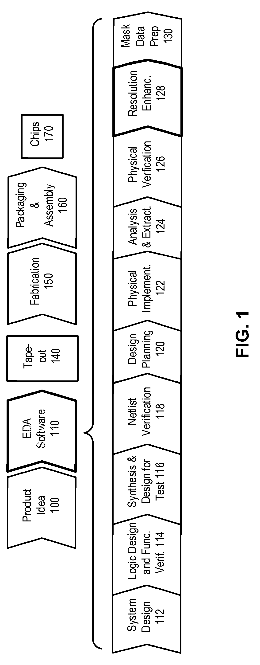
[0027]FIG. 1 illustrates various steps in the design and fabrication of an integrated circuit in accordance with an embodiment of the present invention.

[0028]The process starts with the product idea (step 100) which is realized using an EDA software design process (step 110). When the design is finalized, it can be taped-out (eve...


PUM


Abstract

One embodiment of the present invention provides a system that accurately models polarization effects in an optical lithography system for manufacturing integrated circuits. During operation, the system starts by receiving a polarization-description grid map for a lens pupil in the optical lithography system. The system then constructs a pupil-polarization model by defining a vectorial matrix at each grid point in the grid map, wherein the vectorial matrix specifies a pupil-induced polarization effect on an incoming optical field at the grid point. Next, the system enhances a lithography model for the optical lithography system by incorporating the pupil-polarization model into the lithography / OPC model. The system then uses the enhanced lithography model to perform convolutions with circuit patterns on a mask in order to simulate optical lithography pattern printing.

Description

RELATED APPLICATION[0001]The subject matter of this application is related to the subject matter in a co-pending non-provisional application by the inventors Qiaolin Zhang and Hua Song, and filed on the same day as the instant application entitled, “Modeling an Arbitrarily Polarized Illumination Source in an Optical Lithography System,” having Ser. No. TO BE ASSIGNED, and filing date TO BE ASSIGNED (Attorney Docket No. SNPS-0986-2).BACKGROUND[0002]1. Field of the Invention[0003]The present invention relates to the process of semiconductor manufacturing. More specifically, the present invention relates to a method and an apparatus for accurately modeling polarization state changes for an optical image imposed by a projection lens pupil in an optical lithography system used in a semiconductor manufacturing process.[0004]2. Related Art[0005]Dramatic improvements in semiconductor integration circuit (IC) technology presently make it possible to integrate hundreds of millions of transist...

Claims


Application Information

Patent Timeline
Patent Type & Authority Applications(United States)
IPC IPC(8): G06F17/50
CPCG03F7/70216G03F7/70566G03F7/705G03F7/70441
Inventor ZHANG, QIAOLINSONG, HUALUCAS, KEVIN D.
Owner SYNOPSYS INC
Learn More