Voltage Partitioned Display
a display and voltage technology, applied in the field of large-screen electronic displays, can solve the problems of preventing the production of large-scale display panels formed on continuous substrates, pixel complexity also tends to increase, and achieves the effects of reducing or eliminating voltage disparities across displays, reducing circuit density, and increasing pixel density
- Summary
- Abstract
- Description
- Claims
- Application Information
AI Technical Summary
Benefits of technology
Problems solved by technology
Method used
Image


Examples
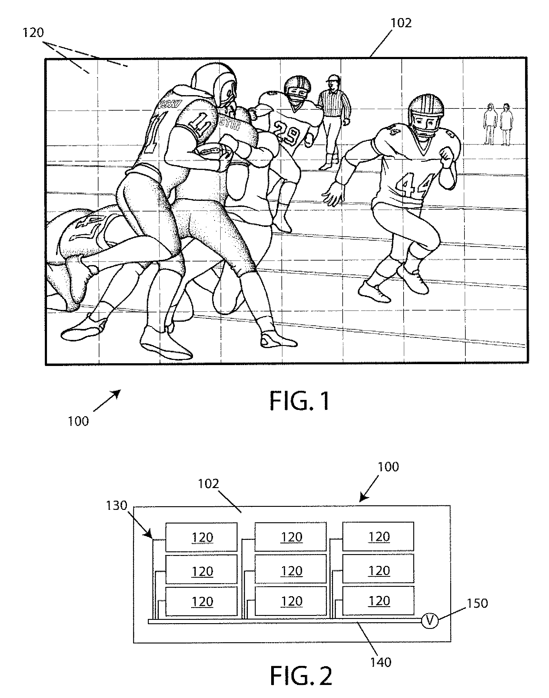
exemplary embodiment 100
[0049]Turning to the figures, wherein like numerals represent like features throughout the views, FIG. 1 shows an exemplary embodiment 100 of a VPD of the present invention. Referring to FIG. 1, the VPD 100 comprises a continuous substrate 102, and a plurality of display subportions 120, each subportion 120 receiving a partitioned voltage from a voltage source (not shown). In an exemplary embodiment, the continuous substrate 102 is a flexible substrate. As shown in FIG. 2, the VPD 100 includes a plurality of subelectrodes 130, each adapted to deliver a voltage to at least one display subportion 120, and a voltage bus 140 electrically coupled to the subelectrodes 130 and adapted to provide a voltage thereto from a voltage source 150. The display subportion 120 and subelectrode 130 can be defined so that the line resistance and capacitance encountered by the subelectrode 130 does not significantly affect the voltage delivered to the subportion 120. As a result, each subportion 120 of ...
exemplary embodiment 400
[0052]FIGS. 4A and 4B show an exemplary embodiment 400 of a VPD of the invention in which a plurality of display elements 408 are formed on a front surface 403 of a substrate 402, and a voltage bus conductor 440 is formed on a rear surface 404 of the substrate 402, As shown in FIG. 4A, the VPD 400 is partitioned into a plurality of display subportions 420, each containing a plurality of display elements 408 and coupled to a subelectrode 430 which comprises a subconductor 432 and subconductor connector 434. Vias 433 are provided to allow electrical connectivity between the front surface 403 of the substrate 402 and the rear surface 404 of the substrate 402. The subconductor 432 on the front surface 403 of the substrate 402 is electrically connected to a subconductor connector 434 on the rear surface 404 through the via 433 to complete the subelectrode 430. FIG. 4B shows the rear surface 404 of the substrate 402 of the VPD 400. As shown in FIG. 4B, the subconductor connector 434 can e...
exemplary embodiment 600
[0063]In a first exemplary embodiment, a data voltage is supplied by a data voltage driver that is electrically coupled to a plurality of display elements. FIG. 6A shows an exemplary embodiment 600 of a VPD of the invention. The VPD 600 includes a plurality of display elements 608 coupled to a front surface 603 of a substrate 602. A data voltage driver 645 is used to supply a data voltage to the display elements 608 in columns 605.
[0064]In an exemplary embodiment, the display element 608 is in the form of a nixel that includes a top electrode layer, preferably formed from a transparent conducting material such as ITO. A transparent insulating layer can be deposited on the front surface 603 of the substrate 602 in such a manner that the top electrode layers of the display elements 608 are left exposed. Leads 615 can be formed over the insulating layer to extend from the top electrode of each display element 608 to a pad (not shown) which provides electrical connectivity between the l...
PUM
 Abstract
Description
Claims
Application Information
 - R&D
- Intellectual Property
- Life Sciences
- Materials
- Tech Scout
- Unparalleled Data Quality
- Higher Quality Content
- 60% Fewer Hallucinations
Browse by: Latest US Patents, China's latest patents, Technical Efficacy Thesaurus, Application Domain, Technology Topic, Popular Technical Reports.
© 2025 PatSnap. All rights reserved.Legal|Privacy policy|Modern Slavery Act Transparency Statement|Sitemap|About US| Contact US: help@patsnap.com