Micro-oscillation element and array of micro-oscillation elements
- Summary
- Abstract
- Description
- Claims
- Application Information
AI Technical Summary
Benefits of technology
Problems solved by technology
Method used
Image
Examples
first embodiment
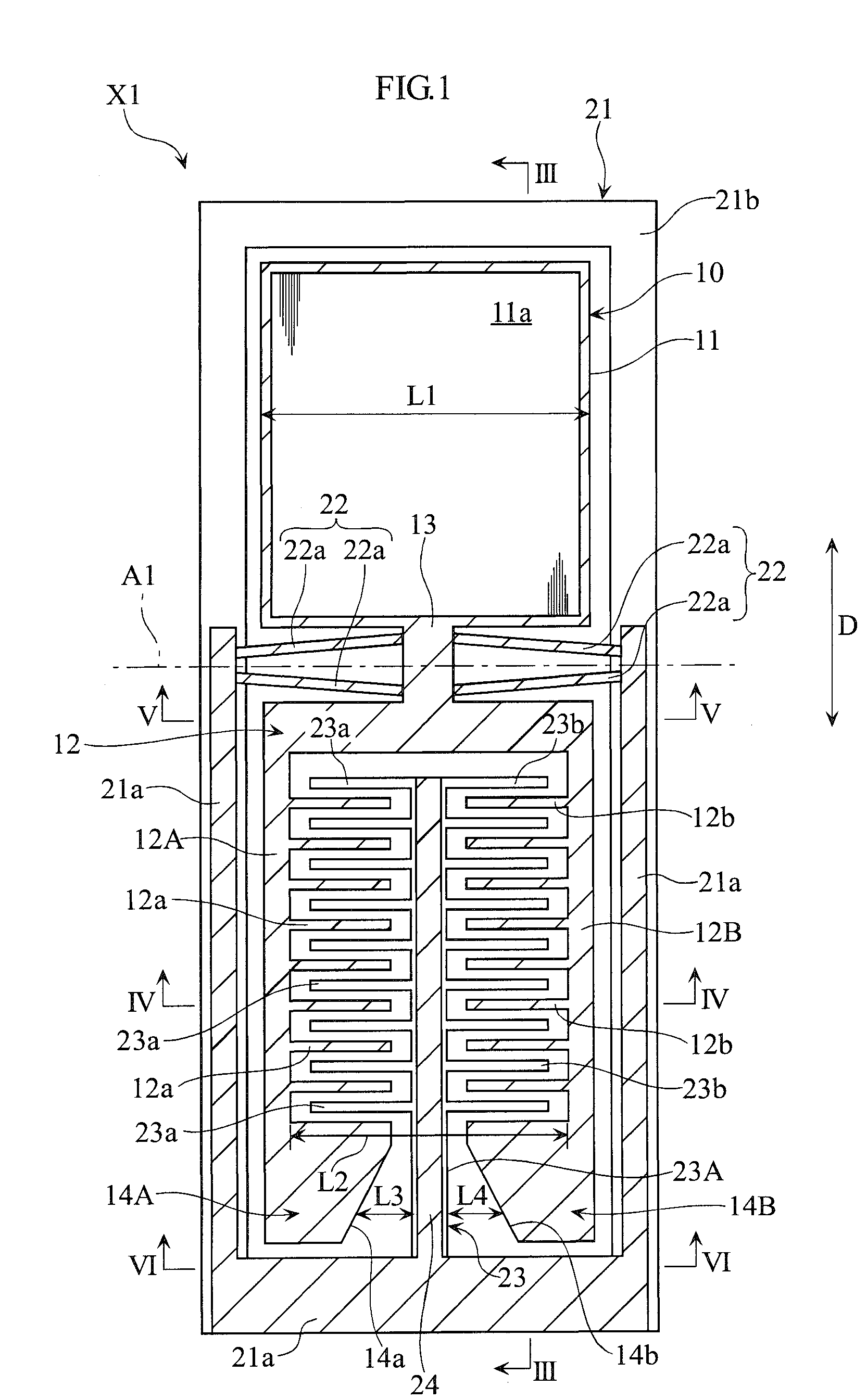
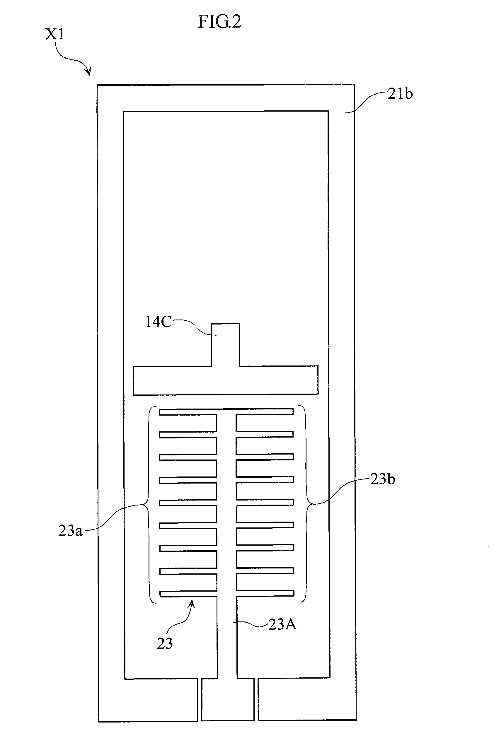
[0050]FIGS. 1 to 6 depict a micro-oscillation element X1 according to the present invention. FIG. 1 is a plan view showing the micro-oscillation element X1; FIG. 2 is a fragmentary plan view of the micro-oscillation element X1; and FIG. 3 is a cross-sectional view taken along a line III-III in FIG. 1. FIGS. 4 to 6 are enlarged cross-sectional views taken along a line IV-IV, V-V, and VI-VI in FIG. 1, respectively.
[0051]The micro-oscillation element X1 includes an oscillating portion 10, a base frame 21, a pair of link portions 22, a driving electrode 23, and a shield electrode portion 24, and is built up as a micromirror element in this embodiment. The micromirror element X1 is herein assumed to be manufactured through processing a material substrate which is so called a silicon-on-insulator (SOI) wafer, by a bulk micromachining technique such as a MEMS technique. The material substrate has a multilayer structure including a first and a second silicon layer, and an insulating layer p...
second embodiment
[0083]FIG. 12 depicts a micro-oscillation element array Y1 according to a FIG. 13 is a fragmentary cross-sectional view taken along a line XIII-XIII in FIG. 12, showing a part of the micro-oscillation element array Y1.
[0084]The micro-oscillation element array Y1 includes a plurality (four in this embodiment) of micro-oscillation elements X1. In the micro-oscillation element array Y1, the plurality of micro-oscillation elements X1 is aligned in a row (one-dimensionally) along the direction of the axis A1. Accordingly, in the micro-oscillation element array Y1, a plurality of mirror portions 11a is aligned in a row along the direction of the axis A1.
[0085]In the micro-oscillation element array Y1, the first layered structure 21a of the frame 21 is continuous throughout all the micro-oscillation elements X1, and hence the driving electrode 12, the weight portion 14C of the oscillating portion 10, the first layered structure 21a and the second layered structure 21b of the frame 21, and...
third embodiment
[0090]FIG. 14 is a plan view showing a part of a micro-oscillation element array Y2 according to the present invention. The micro-oscillation element array Y2 includes a plurality of micro-oscillation elements X2. In the micro-oscillation element array Y2, the plurality of micro-oscillation elements X2 is aligned in a row (one-dimensionally).
[0091]FIGS. 15 to 20 depict the micro-oscillation element X2 constituting the micro-oscillation element array Y2. FIG. 15 is a plan view of the micro-oscillation element X2, and FIG. 16 is a fragmentary plan view thereof. FIGS. 17 to 20 are cross-sectional views taken along a line XVII-XVII, XVIII-XVIII, XIX-XIX, and XX-XX in FIG. 15, respectively.
[0092]The micro-oscillation element X2 includes the oscillating portion 10, a frame 21′, the pair of link portions 22, the driving electrode 23, the shield electrode portion 24, a frame 31, a pair of link portions 32A, 32B, driving electrodes 33, 34, and shield electrode portions 35, 36, 37, and is bui...
PUM
 Abstract
Description
Claims
Application Information
 - R&D
- Intellectual Property
- Life Sciences
- Materials
- Tech Scout
- Unparalleled Data Quality
- Higher Quality Content
- 60% Fewer Hallucinations
Browse by: Latest US Patents, China's latest patents, Technical Efficacy Thesaurus, Application Domain, Technology Topic, Popular Technical Reports.
© 2025 PatSnap. All rights reserved.Legal|Privacy policy|Modern Slavery Act Transparency Statement|Sitemap|About US| Contact US: help@patsnap.com


