Method for depositing thin films by mixed pulsed CVD and ald

Active Publication Date: 2008-12-25
ASM INTERNATIONAL
View PDF63 Cites 444 Cited by
  • Summary
  • Abstract
  • Description
  • Claims
  • Application Information

AI Technical Summary

Benefits of technology

[0003]ALD, in which temporally alternating and sequential reactant pulses of reactants are flowed into a reaction chamber, can be used to form multicomponent films, that is, films composed of thinner constituent films which have different composit

Problems solved by technology

However, it has been found that ALD can have difficulties forming films having some desired compositions.
After an initial cycle of SiCl4 followed by H2O, additional and subsequent SiCl4/H2O cycles were found to result in limited additional deposition.
Moreover, attempting to increase the amount of silicon in the HfSiO film by extending the length of the SiCl4 pulses had little effect.
Thus, these difficulties place severe constraints on the silicon concentrations that can be achieved in HfSiO films that are deposited by ALD.
In another example, when growing HfSiON films using HfCl4, SiCl4, NH3 and H2O as precursors in various ALD sequences, it was difficult to achieve nitrogen concentrations of 3 atomic % or higher.
Without being limited by theory, it is believed that the nitride deposition utilizes a less effective chemistry than the deposition of the other film materials, thereby limiting the nitrogen concentration, since less material is deposited by this chemistry.
It is also believed that

Method used


Image

  • Method for depositing thin films by mixed pulsed CVD and ald
  • Method for depositing thin films by mixed pulsed CVD and ald
  • Method for depositing thin films by mixed pulsed CVD and ald

Examples


example 1

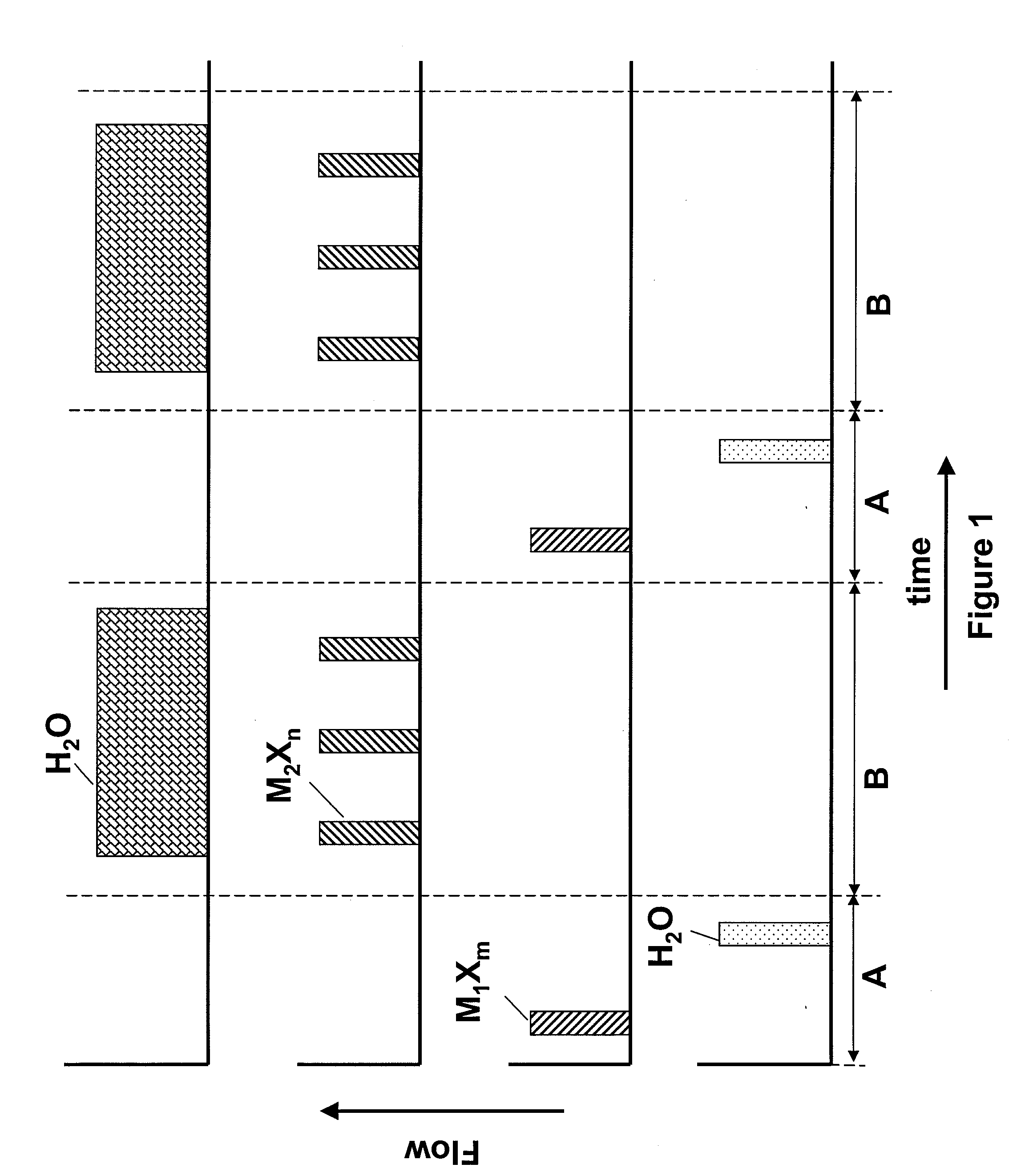
[0042]A hafnium silicate layer is deposited using pulses of HfCl4, SiCl4 and H2O as reactants at a temperature of about 350° C. The sequence as shown in FIG. 1 is applied, where M1Xm, the first metal halide, is HfCl4 and M2Xn, the second metal halide, is SiCl4. The number of SiCl4 pulses is selected to achieve a desired silicon content.

example 2

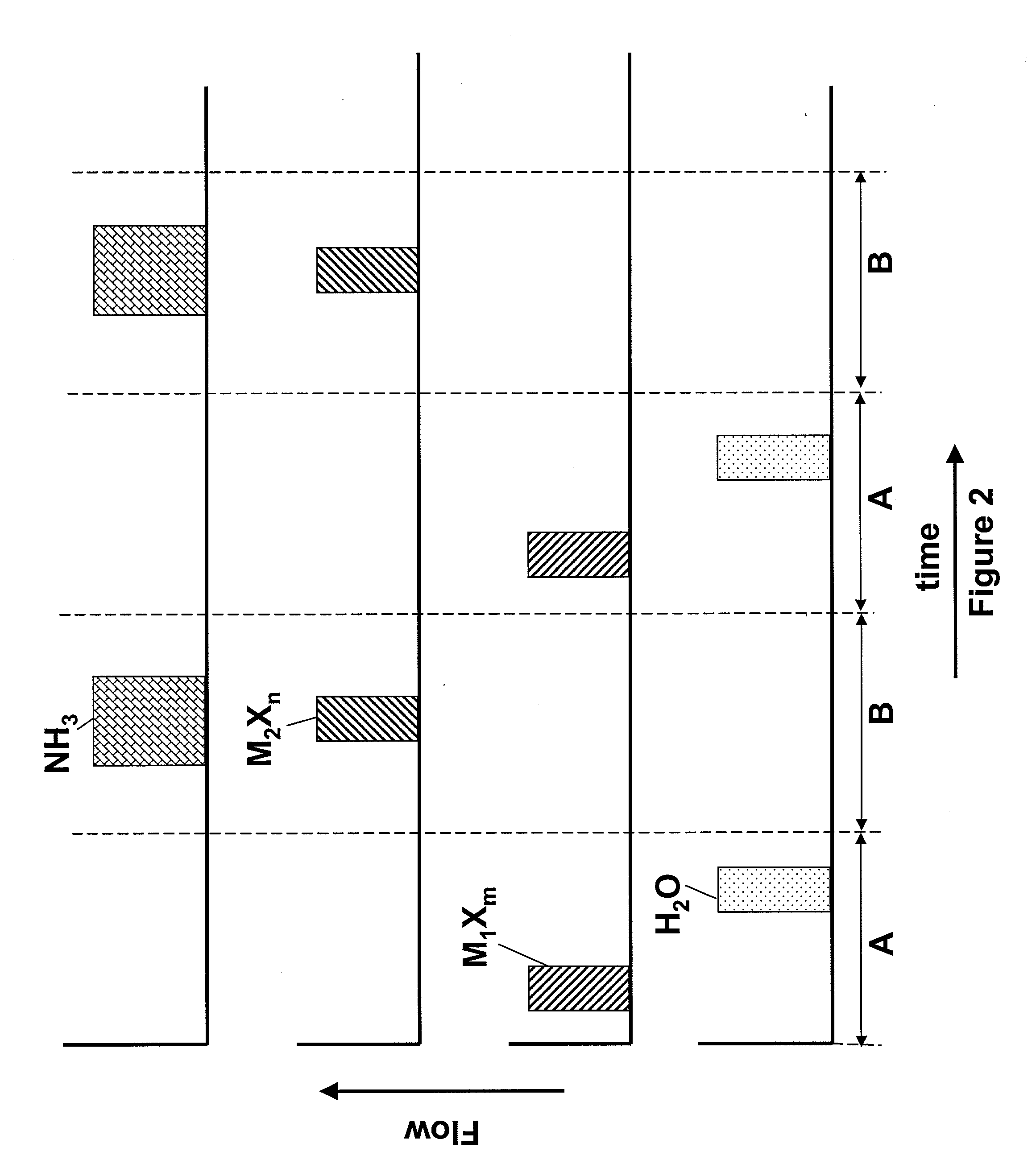
[0043]A hafnium silicon oxynitride layer is deposited using pulses of HfCl4, SiCl4, NH3 and H2O as reactants. The sequence of FIG. 2 is applied, where M1Xm, the first metal halide, is HfCl4 and M2Xn, the second metal halide, is SiCl4. The length of the pulses in period B is tuned to achieve the desired silicon and nitrogen content. The deposition temperature is about 350° C.

[0044]Alternatively, HfCl4 and SiCl4 are mixed and pulses of the mixture are flowed into a reaction chamber with pulses of an oxidant in an ALD mode of operation during a period A and pulses of the mixture are flowed into the reaction chamber with NH3 in a pulsed CVD mode of operation during a period B.

example 3

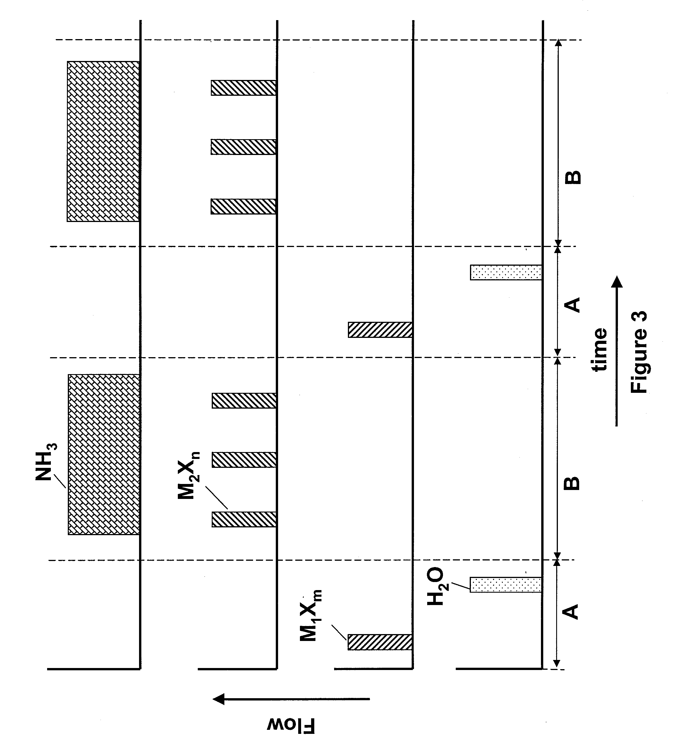
[0045]Hafnium oxide layers are deposited using HfCl4 as the Hf source material. The sequence of FIG. 3 is followed, wherein a first nucleation layer is deposited using HfCl4 and H2O in an ALD mode of processing. Then the remainder of the film is deposited by flowing a plurality of pulses of HfCl4 along with a continuous flow of O3 into the reactor. In this example, the first and second metal are the same and are both Hf. The deposition of the hafnium oxide layers in the pulsed CVD mode of operation may be periodically alternated with one or more cycles of hafnium oxide deposited using the ALD mode of operation.


PUM

PropertyMeasurementUnit
Flow rateaaaaaaaaaa

Abstract

Films are deposited on a substrate by a process in which atomic layer deposition (ALD) is used to deposit one layer of the film and pulsed chemical vapor deposition (CVD) is used to deposit another layer of the film. During the ALD part of the process, a layer is formed by flowing sequential and alternating pulses of mutually reactive reactants that deposit self-limitingly on a substrate. During the pulsed CVD part of the process, another layer is deposited by flowing two CVD reactants into a reaction chamber, with at least a first of the CVD reactants flowed into the reaction chamber in pulses, with those pulses overlapping at least partially with the flow of a second of the CVD reactants. The ALD and CVD parts of the process ca be used to deposit layers with different compositions, thereby forming, e.g., nanolaminate films. Preferably, high quality layers are formed by flowing the second CVD reactant into the reaction chamber for a longer total duration than the first CVD reactant. In some embodiments, the pulses of the third reactant at separated by a duration at least about 1.75 times the length of the pulse. Preferably, less than about 8 monolayers of material are deposited per pulse of the first CVD reactant.

Description

REFERENCE TO RELATED APPLICATION[0001]This application is related to U.S. patent application Ser. No. ______ to Wei-Min Li, filed Jun. 21, 2007, entitled LOW RESISTIVITY METAL CARBONITRIDE THIN FILM DEPOSITION BY ATOMIC LAYER DEPOSITION, Attorney Docket No. ASMMC.075AUS, the entire disclosure of which is incorporated by reference herein.FIELD OF THE INVENTION[0002]The invention relates generally to semiconductor fabrication and, more particularly, to the deposition of thin films onto a substrate by exposing the substrate to mutually reactive reactants in a pulse-wise manner.BACKGROUND AND SUMMARY OF THE INVENTION[0003]ALD, in which temporally alternating and sequential reactant pulses of reactants are flowed into a reaction chamber, can be used to form multicomponent films, that is, films composed of thinner constituent films which have different compositions, and in which the thinner films are preferably vertically stacked in a repeating, regular sequence. By selecting the sequence...

Claims


Application Information

Patent Timeline
IPC IPC(8): H05H1/24
CPCC23C16/18C23C16/30C23C16/308C23C16/34C23C16/401C23C16/405C23C16/45523H01L21/205
Inventor HENDRIKS, MENSOKNAPP, MARTINHAUKKA, SUVI
Owner ASM INTERNATIONAL
Why Eureka
Try Eureka