Delay circuit and delay time adjustment method
a delay time and delay technology, applied in the field of delay circuit and delay time adjustment method, can solve the problems of inability to change the delay time later, disadvantageous inserting a meander pattern to adjust the delay time, and difficult miniaturization of the semiconductor integrated circuit package, so as to achieve easy adjustment and change the delay time. , the effect of high density mounting
- Summary
- Abstract
- Description
- Claims
- Application Information
AI Technical Summary
Benefits of technology
Problems solved by technology
Method used
Image

Examples
first embodiment
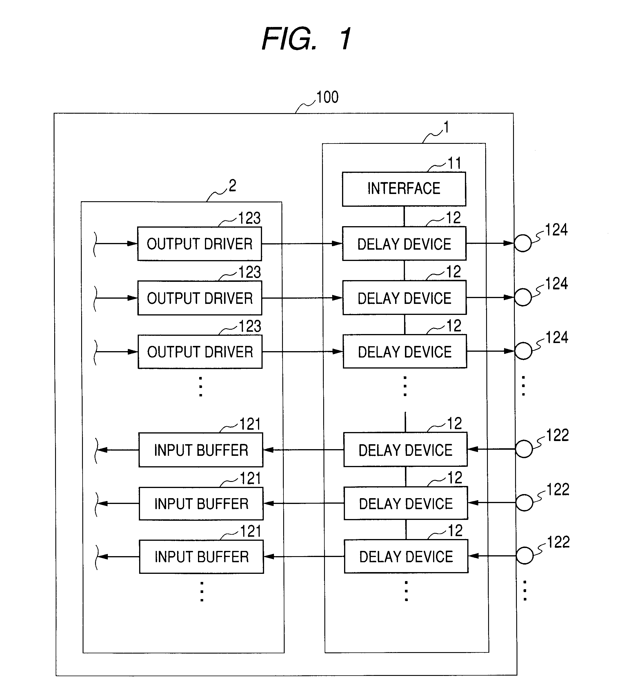
[0066]FIG. 1 is a drawing to show a mount example of a delay circuit according to the invention on a wiring board. In FIGS. 1 to 3, wiring to set a delay time provided on the wiring board will be discussed collectively as wiring for connecting semiconductor chips on the wiring board.
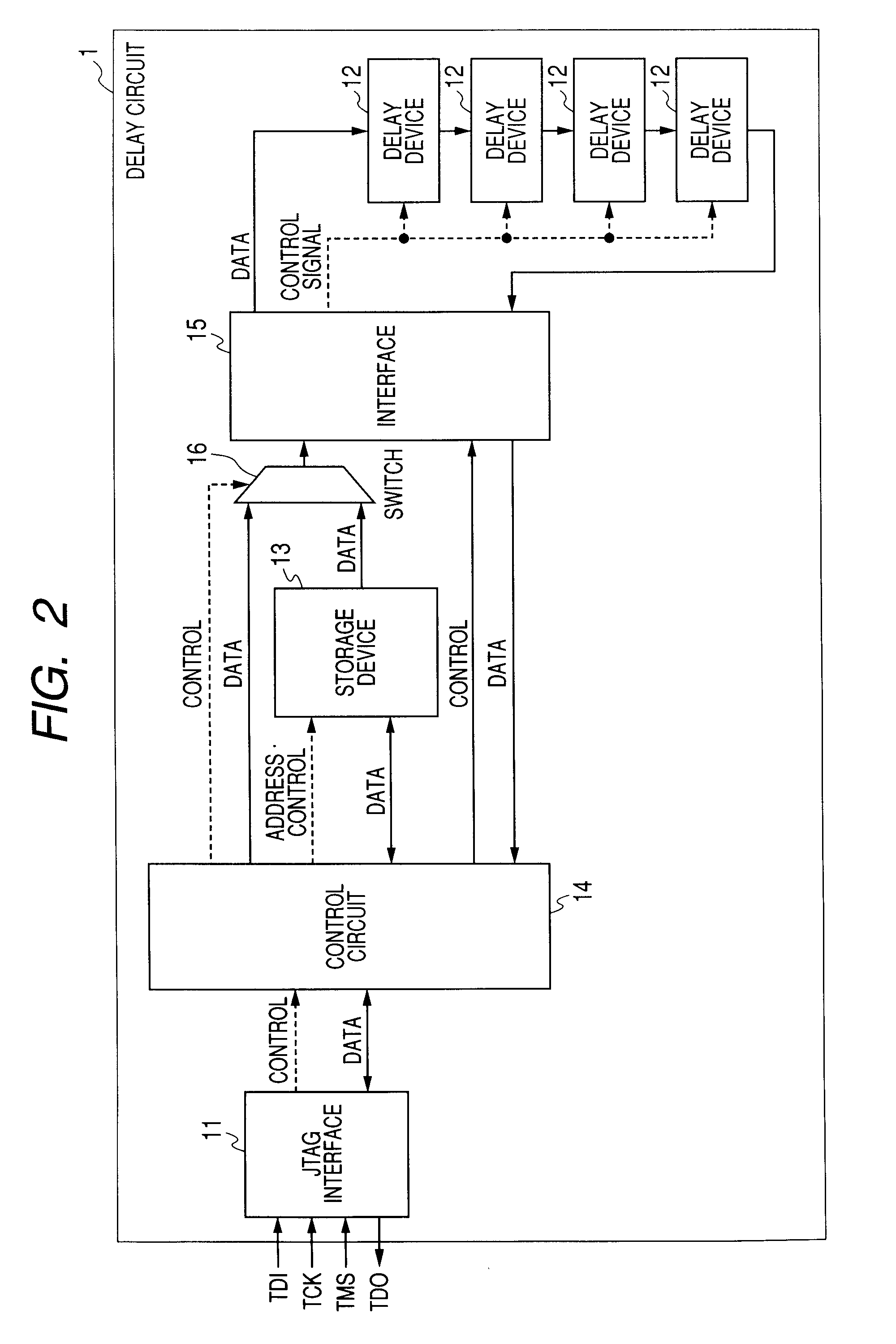
[0067]A delay circuit 1 according to the first embodiment of the invention includes an interface 11 for giving a command of setting a delay time and delay devices 12 that can be set to any desired delay time, and the delay time of the delay device 12 is set according to a command from the interface 11. The interface 11 is a JTAG (Joint Test Action Group) interface. The JTAG is the standard of Boundary Scan Test, one of IC chip inspection methods. In the Boundary Scan Test in the JTAG, TAP (Test Access Port) terminals of the ICs to be inspected are daisy-chained and a plurality of Ices can be read in order for inspection.
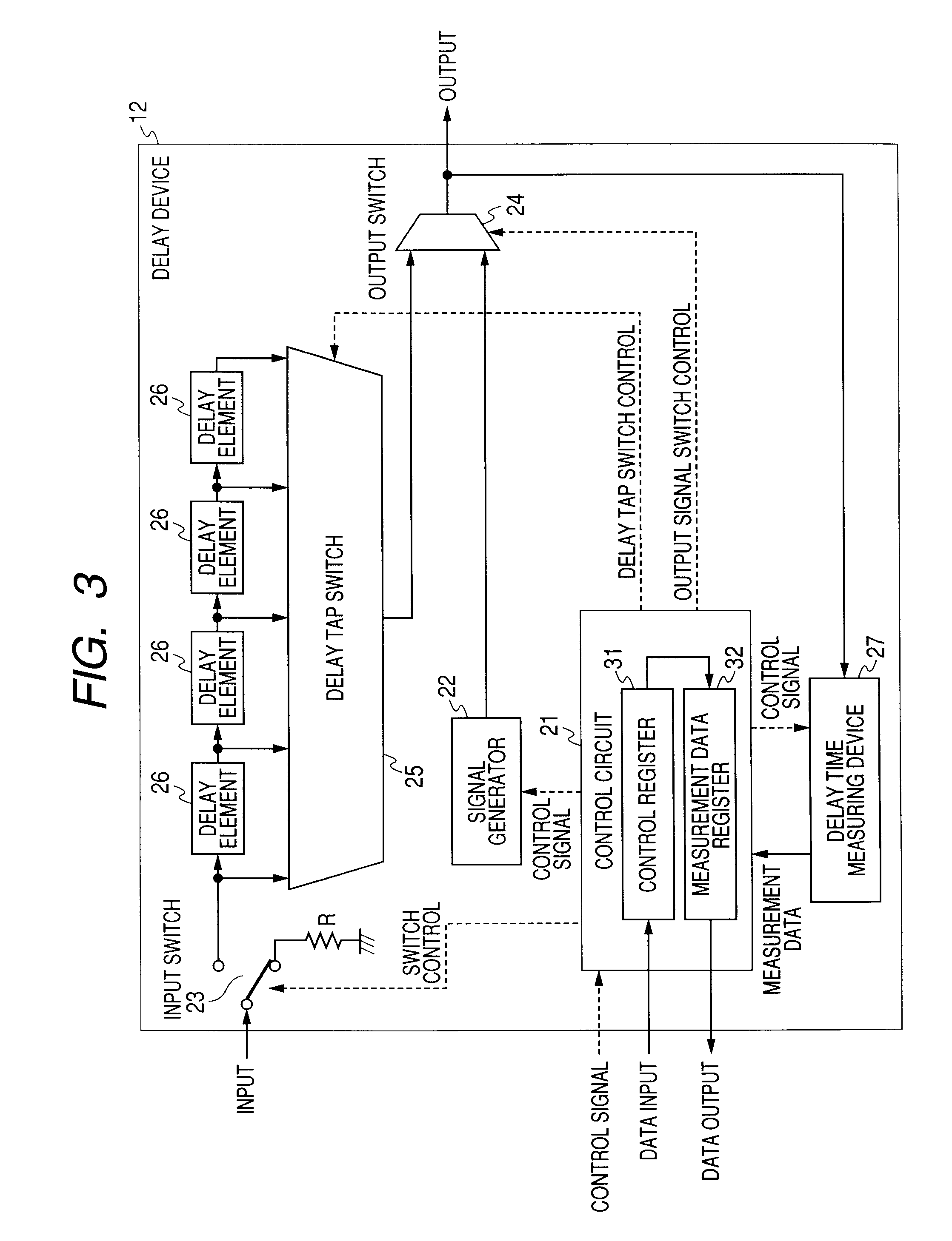
[0068]The delay devices 12 are connected in series by a JTAG chain. If a circuit for ...
second embodiment
[0107]A delay circuit 1 according to the invention includes an interface 11 for giving a command of setting a delay time, input delay devices 12-1 and output delay devices 12-2 that can be set to any desired delay time, and measuring devices 17 for measuring the signal propagation time of measuring reference wiring provided on a wiring board to set the delay time.
[0108]The delay time of each of the input delay devices 12-1 and the output delay devices 12-2 is set according to a command from the interface 11 as in the first embodiment of the invention. The interface 11 is a JTAG (Joint Test Action Group) interface. Measurement data of the measuring device 17 described later in detail (in this case, the signal propagation time of measuring reference wiring) can also be read through the interface 11. The input delay devices 12-1, the output delay devices 12-2, and the measuring devices 17 are connected in series by a JTAG chain.
[0109]Each of the input delay devices 12-1 and the output ...
PUM
 Abstract
Description
Claims
Application Information
 - R&D
- Intellectual Property
- Life Sciences
- Materials
- Tech Scout
- Unparalleled Data Quality
- Higher Quality Content
- 60% Fewer Hallucinations
Browse by: Latest US Patents, China's latest patents, Technical Efficacy Thesaurus, Application Domain, Technology Topic, Popular Technical Reports.
© 2025 PatSnap. All rights reserved.Legal|Privacy policy|Modern Slavery Act Transparency Statement|Sitemap|About US| Contact US: help@patsnap.com