Pattern defect inspection apparatus and method
- Summary
- Abstract
- Description
- Claims
- Application Information
AI Technical Summary
Benefits of technology
Problems solved by technology
Method used
Image
Examples
first embodiment
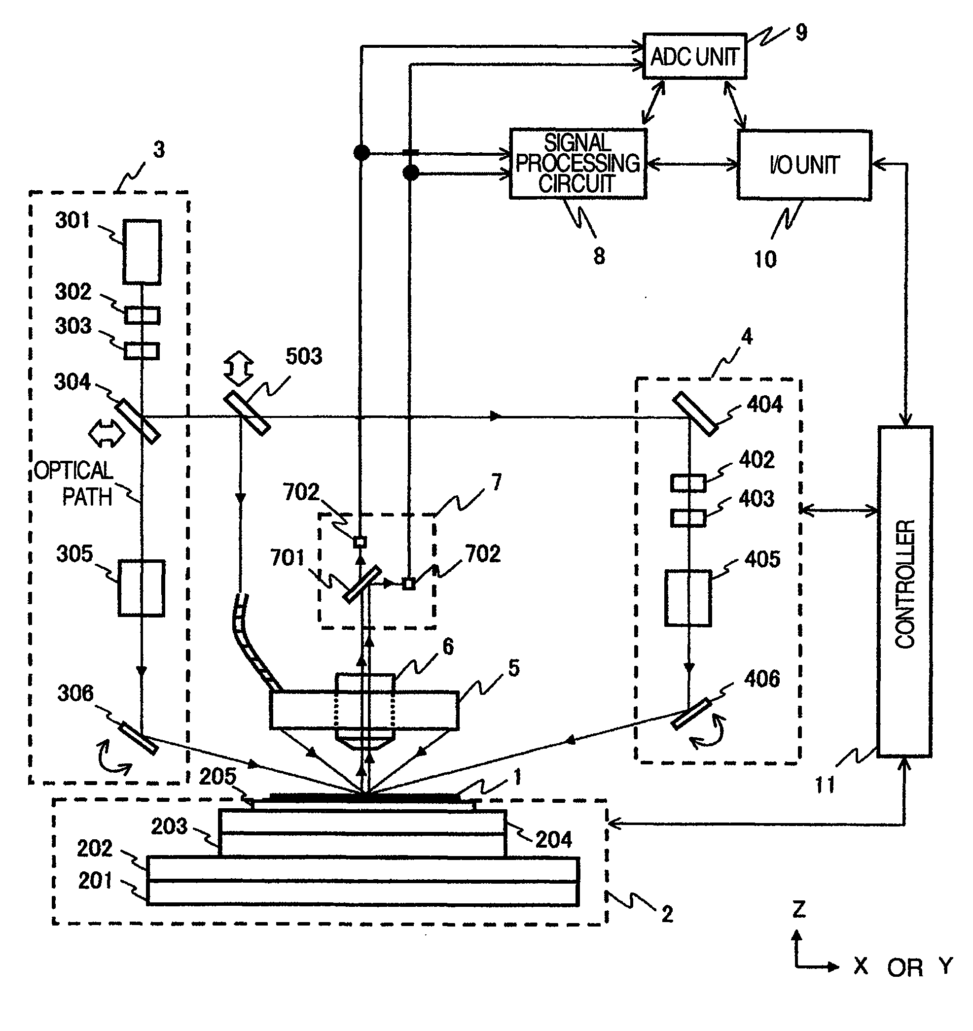
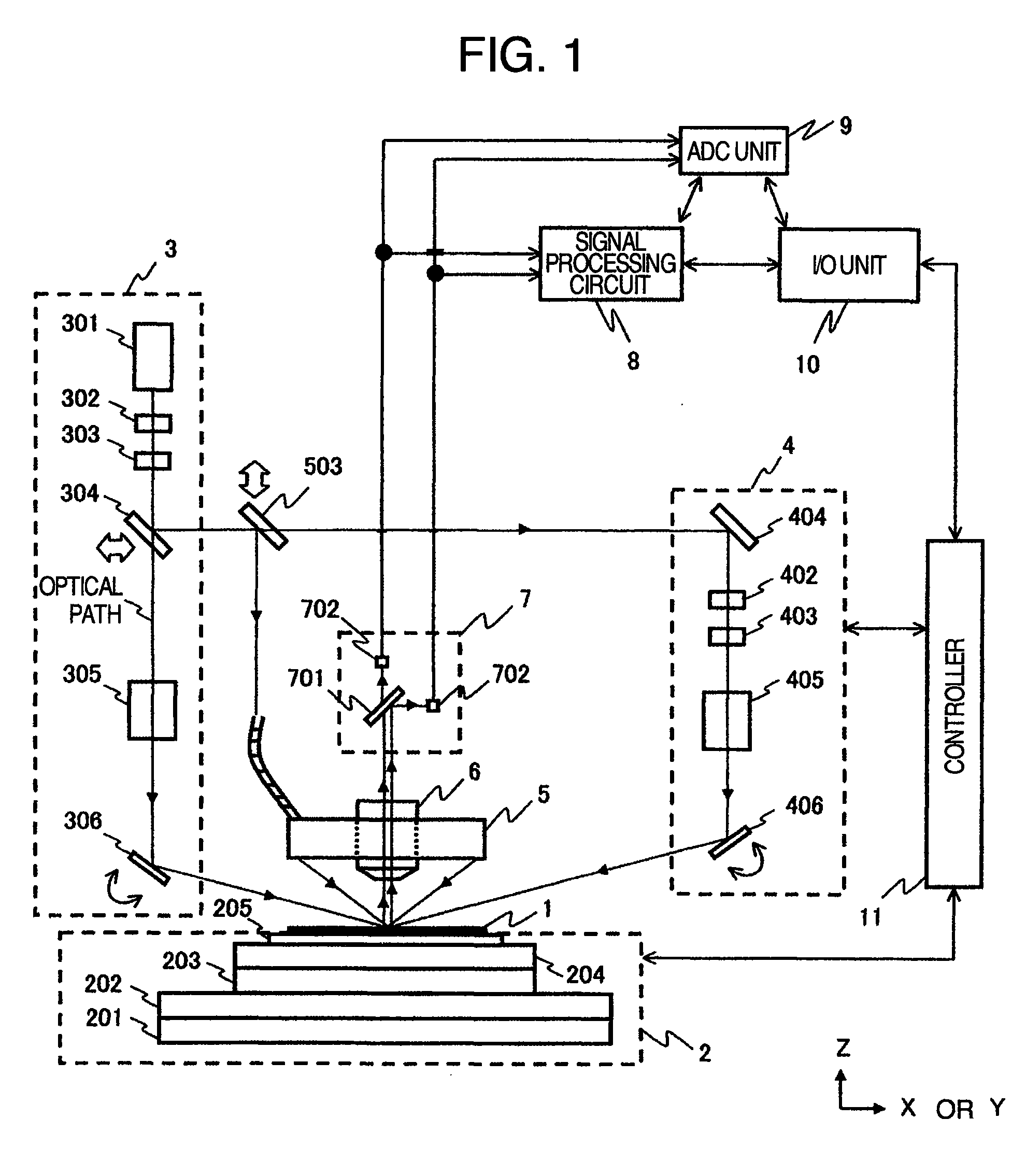
[0046]FIG. 1 is a schematic structural view of a pattern defect inspection apparatus according to the first embodiment of the invention. The invention will be hereinafter explained about the case where it is applied to the inspection of a semiconductor wafer by way of example.
[0047]Referring to FIG. 1, the pattern defect inspection apparatus includes a conveying system 2 for supporting and moving a wafer 1 as an inspection object, illuminating units 3 and 4, a multi-direction illuminating unit 5, an objective lens 6, a multi-region detecting unit 7, a signal processing circuit 8, an ADC (Automatic Defect Classification) unit 9, an input / output unit 10, a controller 11 for each unit and relay lenses and mirrors that are not shown in the drawing. Incidentally, arrows (part of which is not shown) extending from the controller 11 to each unit represents that control signals, etc, are mutually communicated.
[0048]Next, the operation will be explained. Beams of illumination light emitted f...
second embodiment
[0101]Next, the second embodiment of the invention will be explained. In this second embodiment, the construction of the illuminating units 3 and 4 of the defect inspection apparatus is different from the construction in the first embodiment. Since the rest of the constructions are the same, their detailed explanation will be omitted.
[0102]FIG. 13 shows the construction of the illumination of the second embodiment for illuminating a plurality of regions on the wafer 1. The difference of the example shown in FIG. 13 from that of FIG. 2 resides in that whereas illumination is made from if directions with respect to the X or Y direction of the conveying system 2 in the example shown in FIG. 2, it is made from the same direction, that is, from the direction of f=0 in the example shown in FIG. 13.
[0103]The advantage of the construction of the illuminating unit shown in FIG. 13 is that the size of the construction of the apparatus can be reduced because the illumination direction and the ...
third embodiment
[0105]Next, the third embodiment of the invention will be explained. In the third embodiment, the construction of the illuminating unit 3 of the defect inspection apparatus is different from the construction in the first embodiment. Since the rest of the constructions are the same, their detailed explanation will be omitted.
[0106]FIG. 14 shows a schematic construction of the illuminating unit in this third embodiment. The third embodiment uses a plurality of light sources of the illuminating unit. In FIG. 14, an illumination light source 3401 of a wavelength λ2 different from the wavelength λ1 of the illumination light source 301, a light power polarization adjusting unit 3402, a coherency reducing unit 3403, a condensation optical system 3405 and an oblique illumination mirror 3406 are arranged in place of the illuminating unit 4.
[0107]The functions of the light power polarization adjusting unit 3402, the coherency reducing unit 3403, the condensation optical system 3405 and the ob...
PUM
 Abstract
Description
Claims
Application Information
 - R&D
- Intellectual Property
- Life Sciences
- Materials
- Tech Scout
- Unparalleled Data Quality
- Higher Quality Content
- 60% Fewer Hallucinations
Browse by: Latest US Patents, China's latest patents, Technical Efficacy Thesaurus, Application Domain, Technology Topic, Popular Technical Reports.
© 2025 PatSnap. All rights reserved.Legal|Privacy policy|Modern Slavery Act Transparency Statement|Sitemap|About US| Contact US: help@patsnap.com


