
Tri-State Circuit Element Plus Tri-State-Multiplexer Circuitry

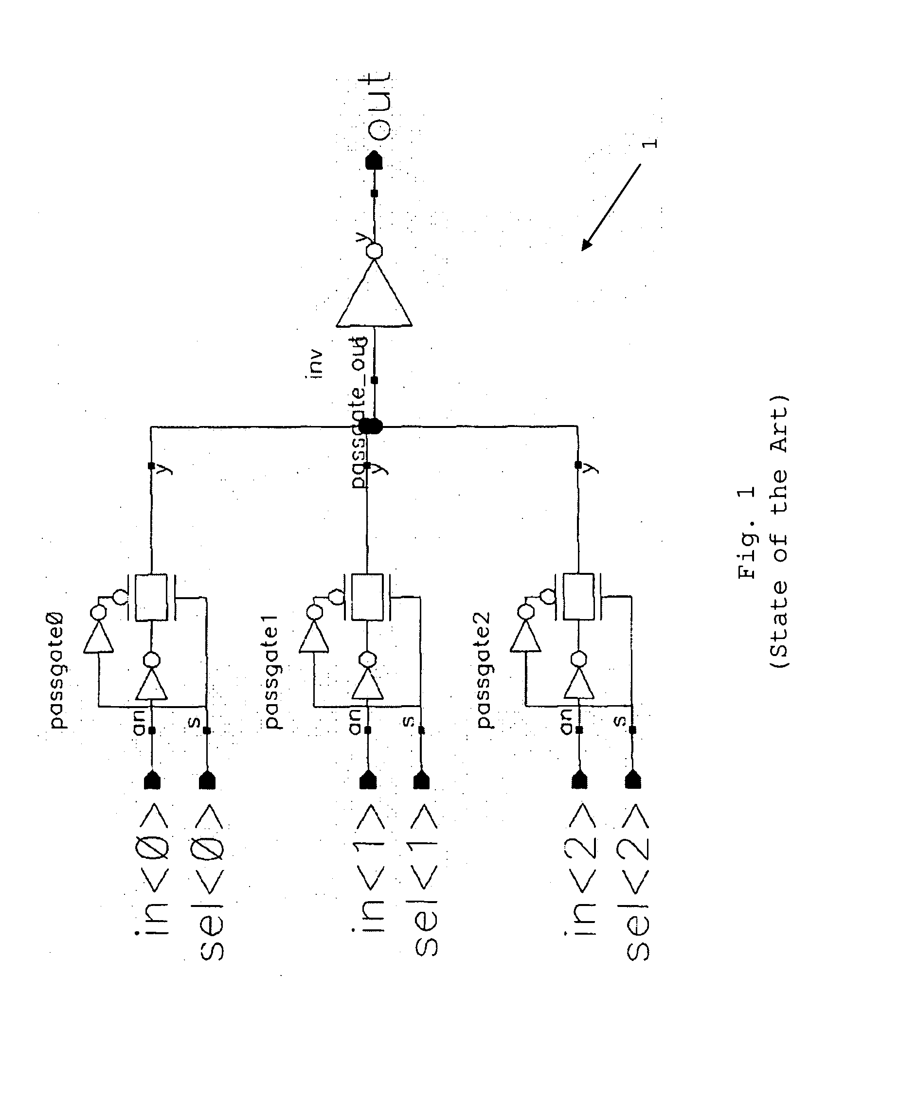
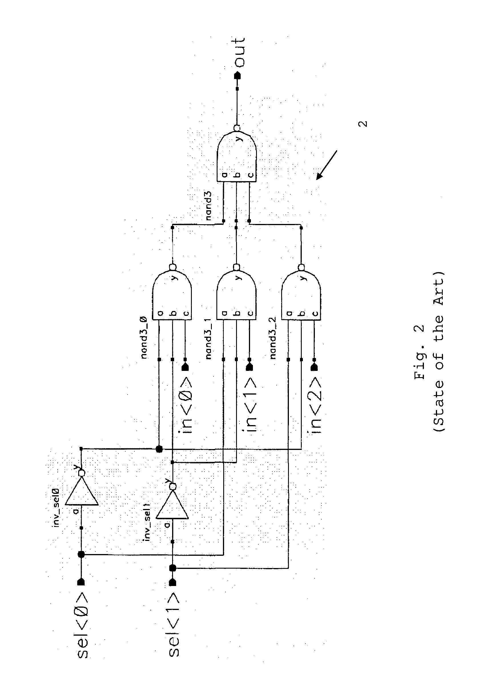
a circuit element and tri-state technology, applied in logic circuits, pulse techniques, electronic switching, etc., can solve the problems of large area requirements, high power consumption, and inability to meet input capacitance and delay time, so as to reduce the set of devices, drive high output loads, and improve performance

Inactive Publication Date: 2008-10-23
IBM CORP
View PDF1 Cites 9 Cited by
  • Summary
  • Abstract
  • Description
  • Claims
  • Application Information

AI Technical Summary

Benefits of technology

[0010]Said Tri-State circuit element according to the invention has the advantage over the state of the art, that it can be used to drive high output loads that are highly constrained on cycle time, i.e. driving high output loads with short gate delay. Regarding the ability to drive high output loads, the Tri-State-Multiplexer circuitry according to the invention has a reduced set of devices and an improved performance compared to a Tri-State-Multiplexer circuitry plus an intermediate circuitry needed for an intermediate amplification according to the state of the art. Further the Tri-State-Multiplexer circuitry according to the invention has very low input capacitances compared to the state of the art Tri-State-Multiplexer circuitries. The Tri-State-Multiplexer circuitry according to the invention further is area optimized due to its reduced set of devices resulting in a reduced power leakage.

Problems solved by technology

This approach is disadvantageous regarding performance, input capacitances and delay time.
Further this approach requires a huge amount of devices, i.e. semi-conductor elements, particularly transistors, within the Tri-State-Multiplexer circuitry and the intermediate circuitries resulting in high power consumption, large area requirement and due to this high power leakage.
This Tri-State circuit element due to its only nine devices has a low area requirement with only a small power leakage but it is too weak to be used to build an on-chip memory's Tri-State-Multiplexer circuitry to directly drive a cache.

Method used


Image

  • Tri-State Circuit Element Plus Tri-State-Multiplexer Circuitry
  • Tri-State Circuit Element Plus Tri-State-Multiplexer Circuitry
  • Tri-State Circuit Element Plus Tri-State-Multiplexer Circuitry

Examples


Embodiment Construction

[0019]A Tri-State circuit element 100 according to the invention is shown in FIG. 6. The Tri-State circuit element 100 is composed of Complementary Metal Oxide Semiconductor (CMOS)—devices, i.e. transistors. The Tri-State circuit element 100 has a data signal input terminal 102 for receiving a data signal, an enable signal input terminal 104 for receiving an enable signal, and an output signal terminal 106 for providing an output signal. The Tri-State circuit element 100 further has a first CMOS transistor 110 of a first conductivity type having a source 111, a drain 112, and a gate 113, said source 111 being connected to a supply voltage VDD, and said drain 112 being connected to said output signal terminal 106. The Tri-State circuit element 100 also has a second CMOS transistor of a second conductivity type opposite to said first conductivity type, said second CMOS transistor having a drain connected to said output signal terminal 106, a source 121 connected to ground and a gate 1...


PUM


Abstract

A Tri-State circuit element (100) composed of Complementary Metal Oxide Semiconductor (CMOS)—devices is described. Said Tri-State circuit element (100) having a data signal input terminal (102) for receiving a data signal, an enable signal input terminal (104) for receiving an enable signal, and an output signal terminal (106) for providing an output signal. Furthermore a Tri-State-Multiplexer circuitry (300) composed of such Tri-State circuit elements (100) is described.

Description

BACKGROUND OF THE INVENTION[0001]The invention relates to a Tri-State circuit element plus a Tri-State-Multiplexer circuitry.[0002]Tri-State-Multiplexer circuitries are well known from the state of the art. Within microprocessors they can be used e.g. to connect small on-chip memories, like e.g. a pre-stage of a cache with a, compared to the on-chip memory relatively large cache memory that can be arranged on- or off-chip. Thereby the Tri-State-Multiplexer circuitry is used to select one single data signal of a small number of data signals of the pre-stage to be forwarded to the cache.[0003]Regarding this utilization of a Tri-State-Multiplexer circuitry, the relatively weak, i.e. small data signal from a selected Tri-State circuit element of the Tri-State-Multiplexer circuitry is available to be used to drive the cache. For maximum performance, the data signal has to be propagated to the cache as fast as possible. Since according to the state of the art the data signal of the on-chi...

Claims


Application Information

Patent Timeline
IPC IPC(8): H03K19/00
CPCH03K17/005H03K19/0002H03K19/0013
Inventor FRANGER, DIRKSAUTTER, ROLFWERNER, TOBIASWITTE, PASCAL
Owner IBM CORP
Learn More