
Product Management System

a product management and product technology, applied in the field of product management systems, can solve the problems of difficult to receive electromagnetic waves, block communication with an id tag attached to each product, and block communication with an id tag using a reader/writer (also referred to as r/w), and achieve the effect of low cost and higher performan

Inactive Publication Date: 2008-09-18
SEMICON ENERGY LAB CO LTD
View PDF21 Cites 32 Cited by
  • Summary
  • Abstract
  • Description
  • Claims
  • Application Information

AI Technical Summary

Benefits of technology

[0006]The present invention has been made in view of the above described problems. It is an object of the present invention to provide a product management system that can secure the stability of communication between an ID tag attached to a product and an R / W, and can conduct management of products simply and efficiently, even if a product is packed by a package body.
[0009]A product management system according to the present invention has a structure described above. Thus, information stored in an ID tag can be surely read and erased, and information can be surely written, overwritten and so on in the ID tag, by conducting reception / transmission of a signal between an R / W and the ID tag through a resonant circuit portion. Specifically, communication disabled or communication instability due to directivity (a property of going in only a certain direction or a property of receiving from only a certain direction) between an R / W and an ID tag attached to a product can be solved and communication between them can be conducted surely. Therefore, the present invention is effective when reading or writing information in an ID tag 2 attached to a product 1 once in a short time.
[0010]An ID tag used in the present invention includes at least a thin film integrated circuit portion including a thin film transistor, and an antenna, and thus can be manufactured at a lower cost than an ID tag formed by a conventional method by which a plurality of integrated circuits are formed over a silicon wafer and the silicon wafer is ground and removed to isolate the thin film integrated circuits. In other words, the thin film integrated circuits can be separated from a substrate on which the plurality of thin film integrated circuits are formed to isolate elements. ID tags can be manufactured at a lower cost since a glass substrate or the like that is less expensive than a silicon wafer can be used as a separation substrate (a substrate from which element are separated) which the separation substrate can also be used multiple times.
[0011]Further, in forming a resonant circuit portion, a plurality of thin film integrated circuit portions mainly having a thin film structure is formed over a substrate, and the resonant circuit portion is formed by the separation method, thereby manufacturing the resonant circuit portion at a low cost.
[0013]As described above, communication between an R / W and an ID tag can be conducted more securely through a resonant circuit portion using an ID tag manufactured at low cost. Therefore, product management system with higher performance can be provided.

Problems solved by technology

At this time, when a product exists in a package body, there is a risk that communication with an ID tag using a reader / writer (also referred to as R / W) is blocked.
In addition, when packing bodies containing products are stacked in a storehouse or the like, communication with an ID tag attached to each product may be blocked.
Specifically, if communication range of an R / W is short, more internal products or products packed by a more internal package body is difficult to receive an electromagnetic wave emitted from the R / W.
Then, it is difficult to manage products in a distribution process of products, which leads to lose convenience of ID tags.

Method used


Image

  • Product Management System
  • Product Management System
  • Product Management System

Examples


embodiment mode 1

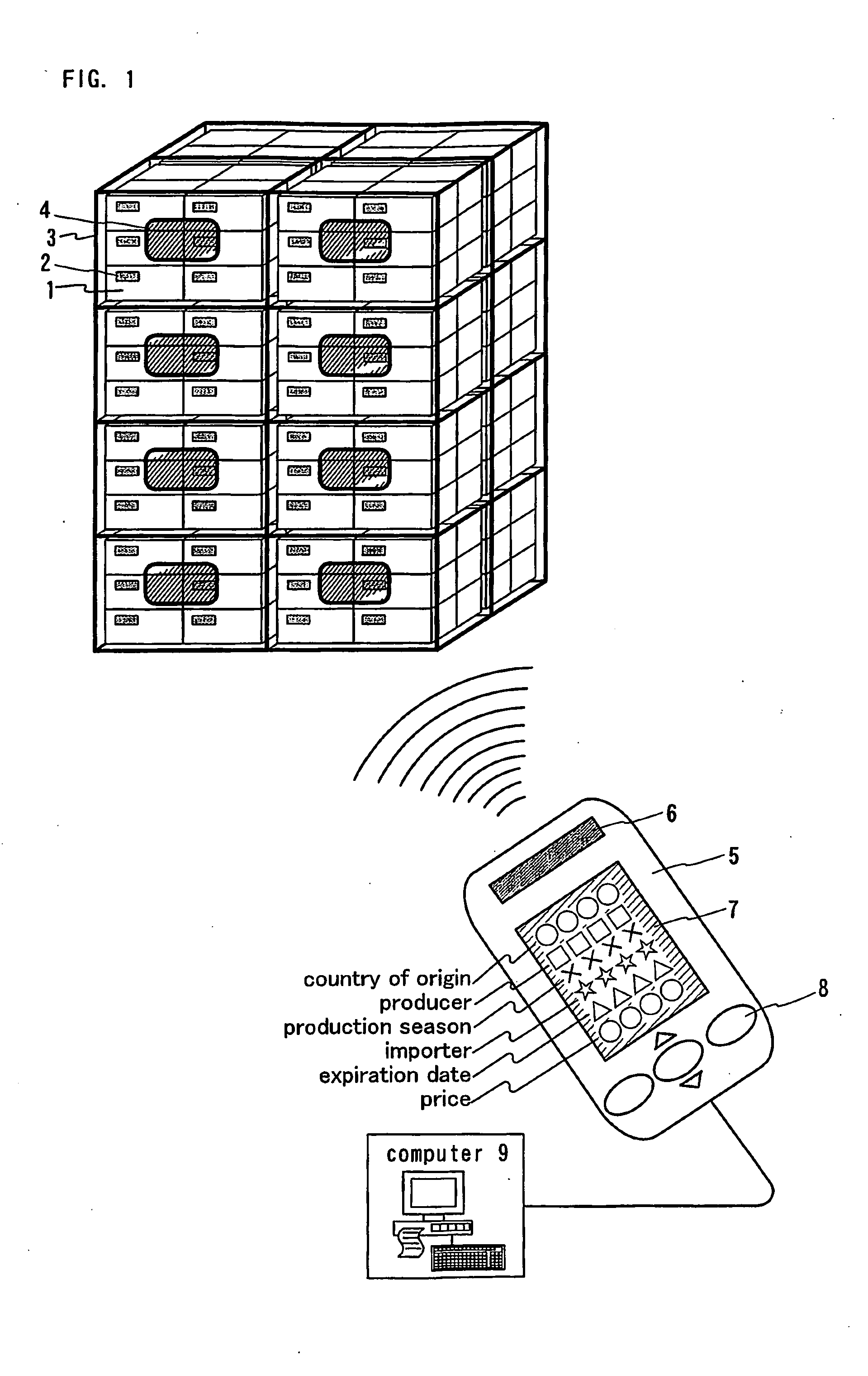
[0029]A structure of a product management system according to the present invention is described with reference to FIG. 1.

[0030]In FIG. 1, a plurality of packing bodies 3 in which products 1 are packed are stacked. An ID tag 2 storing various information about the product 1 is attached to the product 1. A resonant circuit portion 4 is formed in the package body 3. The products 1 may be of the same types or different types.

[0031]Herein, an ID tag (Identification tag) attached to a product has mainly a function of identifying products distributed in a market or a function of storing information on the products, and is referred to as an ID chip, an ID label an ID seal, an ID sticker and the like depending on a mode thereof. ID tags include a card-like ID tag An ID tag in the present invention includes a thin film integrated circuit portion. The thin film integrated circuit portion is conceptually different from a conventional IC (Integrated Circuit) which is formed on a silicon wafer. ...

embodiment mode 2

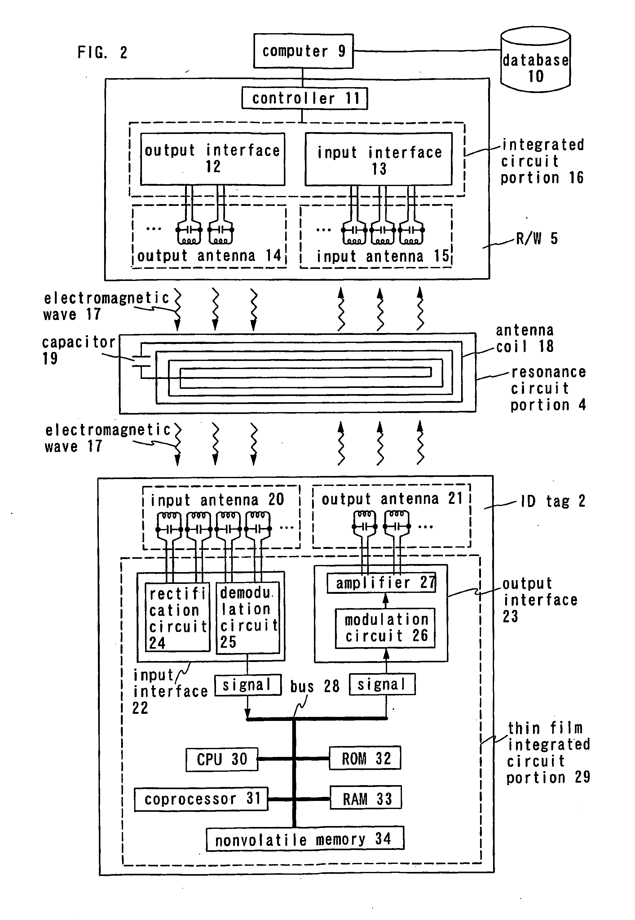
[0045]A product management system according to the present invention is described more in detail with reference to FIG. 2. FIG. 2 is a block diagram showing configurations of an ID tag 2, a resonant circuit portion 4 and an R / W 5.

[0046]The R / W 5 includes at least an output interface 12, an input interface 13, an output antenna 14 and an input antenna 15. Note that the number of each antenna is not limited to that shown in FIG. 2. Moreover, the shape of antenna is not limited to a coil-like shape.

[0047]A signal modulated in the output interface 12 of the R / W 5 is output from the output antenna 14 and sent to the ID tag 2 through the resonant circuit portion 4 provided in a package body 3.

[0048]The resonant circuit portion 4 includes at least a circuit provided with an impedance Z that is inductive and capacitive. The inductive impedance is an inductance Land the capacitive impedance is a capacitance C. For example, as shown in FIG. 2, the resonant circuit portion 4 includes at least ...

embodiment 1

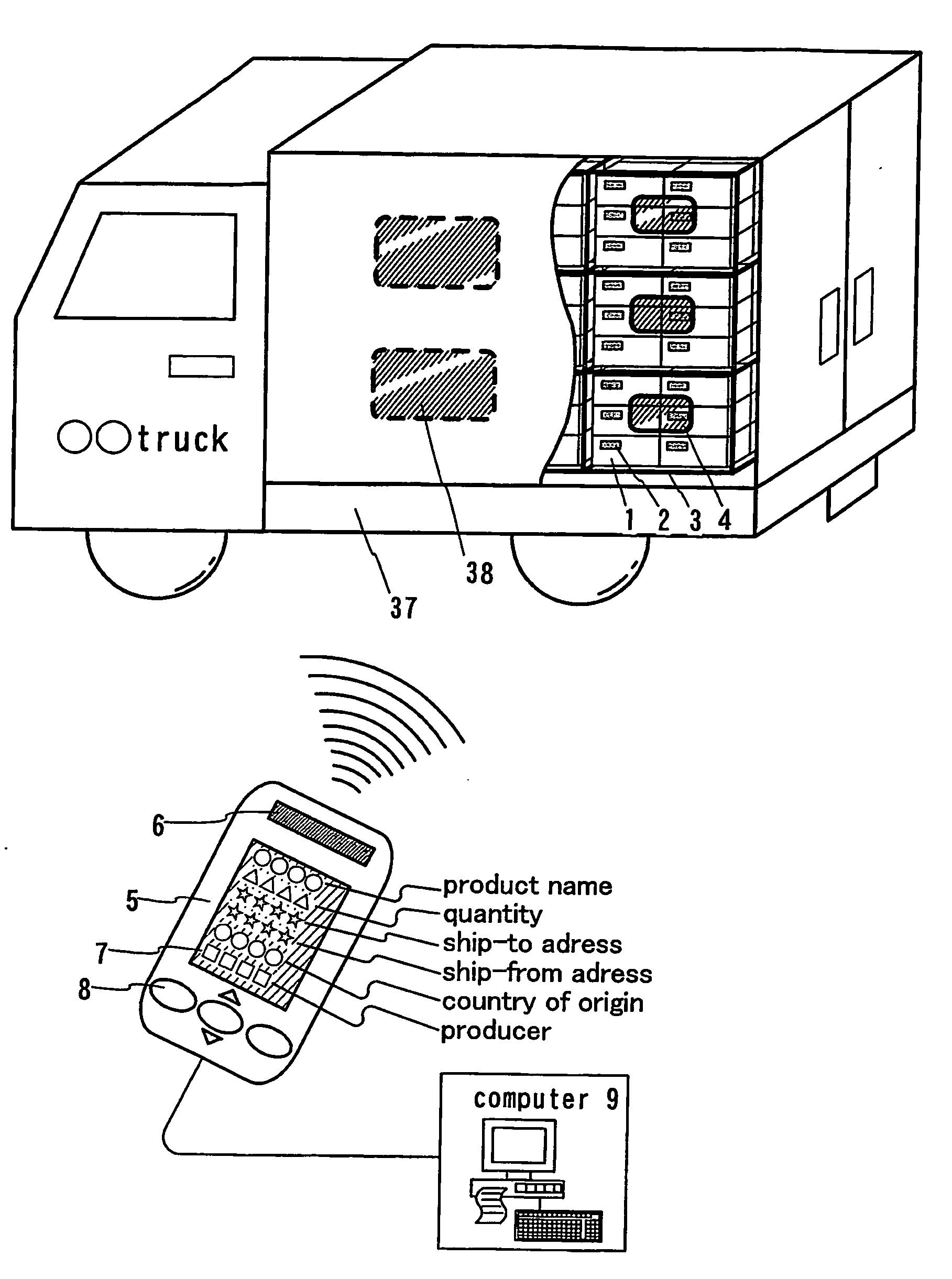
[0067]An example of applying the present invention is described with reference to FIG. 3 in Embodiment 1. Baggage inspection in the airport or the like is shown in FIG. 3. Here, a suitcase 35 of a tourist or the like serves as a package body. The suitcase 35 includes at least one resonant circuit portion 4. The resonant circuit portion 4 may be provided for an outer surface of the suitcase 35; however, is preferably formed inside or an interior portion of a cover for preventing separation due to external force, theft and the like. Inside the suitcase 35, a product 1 and the like are packed. ID tags 2 are attached to each product.

[0068]Baggage such as the suitcase 35 containing the product 1 is transferred by a conveyer 37. When the baggage reaches an antenna portion 6 of the R / W 5, the resonant circuit portion 4 provided for the suitcase 35 receives an electromagnetic wave from the R / W 5 and transmits the electromagnetic wave to the ID tag 2. As described above, the resonant circuit...


PUM


Abstract

When a product attached with an ID tag is placed inside a package body, there is a risk that communication with an ID tag using a reader / writer is blocked. Then, it is difficult to manage products in a distribution process of products, which leads to lose convenience of ID tags. One feature of the present invention is a product management system that includes a package body for packing a product attached with an ID tag, and a reader / writer. The ID tag includes a thin film integrated circuit portion and an antenna, the package body includes a resonance circuit portion having an antenna coil and a capacitor, and the resonance circuit portion can communicate with the reader / writer and the ID tag. Accordingly, the stability of communication between an ID tag attached to a product and an R / W can be secured, and management of products can be conducted simply and efficiently, even if a product is packed by a package body.

Description

TECHNICAL FIELD[0001]The present invention relates to a product management system that reads and writes information about a product attached with an ID tag including a memory, a CPU and the like by a reader / writer.BACKGROUND ART[0002]Recently, in all kinds of industrial worlds such as food industry and manufacturing industry, demands for strengthening safety and management systems of products have been heightened, and therewith, the amount of information on the products are increasing. However, the current information on a product is just information such as a country of manufacture, a manufacturer, or an item number, mainly provided by ten and several figures of a barcode, and the amount of information is quite small. Further, in the case of using a barcode, scanning the barcodes by hand one by one requires long time. Consequently, instead of the barcode system, an automatic recognition technique by a non-contact IC tag utilizing an electromagnetic wave, which is called RFID (Radio...

Claims


Application Information

Patent Timeline
Patent Type & Authority Applications(United States)
IPC IPC(8): H04Q5/22B65G61/00G06K17/00G06K19/00H04B1/59H04B5/02
CPCG06K7/10178G06K17/00G06K19/07758H04B5/0081H04B5/0012H04B5/0056G06K2017/0051H04B5/22H04B5/77H04B5/26
Inventor ARAI, YASUYUKIAKIBA, MAITACHIMURA, YUKOKANNO, YOHEI
Owner SEMICON ENERGY LAB CO LTD
Learn More