Method for manufacturing a field effect transistor with auto-aligned grids

a field effect transistor and grid technology, applied in the manufacturing of semiconductor/solid-state devices, basic electric elements, electric devices, etc., can solve problems such as affecting the operation of the obtained devi

Active Publication Date: 2008-09-11
COMMISSARIAT A LENERGIE ATOMIQUE ET AUX ENERGIES ALTERNATIVES
View PDF8 Cites 1 Cited by
  • Summary
  • Abstract
  • Description
  • Claims
  • Application Information

AI Technical Summary

Benefits of technology

[0016]forming in the layer of front grid material a pattern reproducing the shape of the masking element and comprising the etching of the layer of front grid material so as to eliminate the front grid material outside said pattern,
[0038]According to a second embodiment, the step consisting of forming a pattern in the layer of front grid material comprises a step of anisotropic etching in order to eliminate the front grid material outside the pattern.

Problems solved by technology

Another disadvantage inherent to these methods is that the capacitances present between the front grid and the source and between the front grid and the drain can impair the functioning of the device obtained.

Method used


Image

  • Method for manufacturing a field effect transistor with auto-aligned grids
  • Method for manufacturing a field effect transistor with auto-aligned grids
  • Method for manufacturing a field effect transistor with auto-aligned grids

Examples


Embodiment Construction

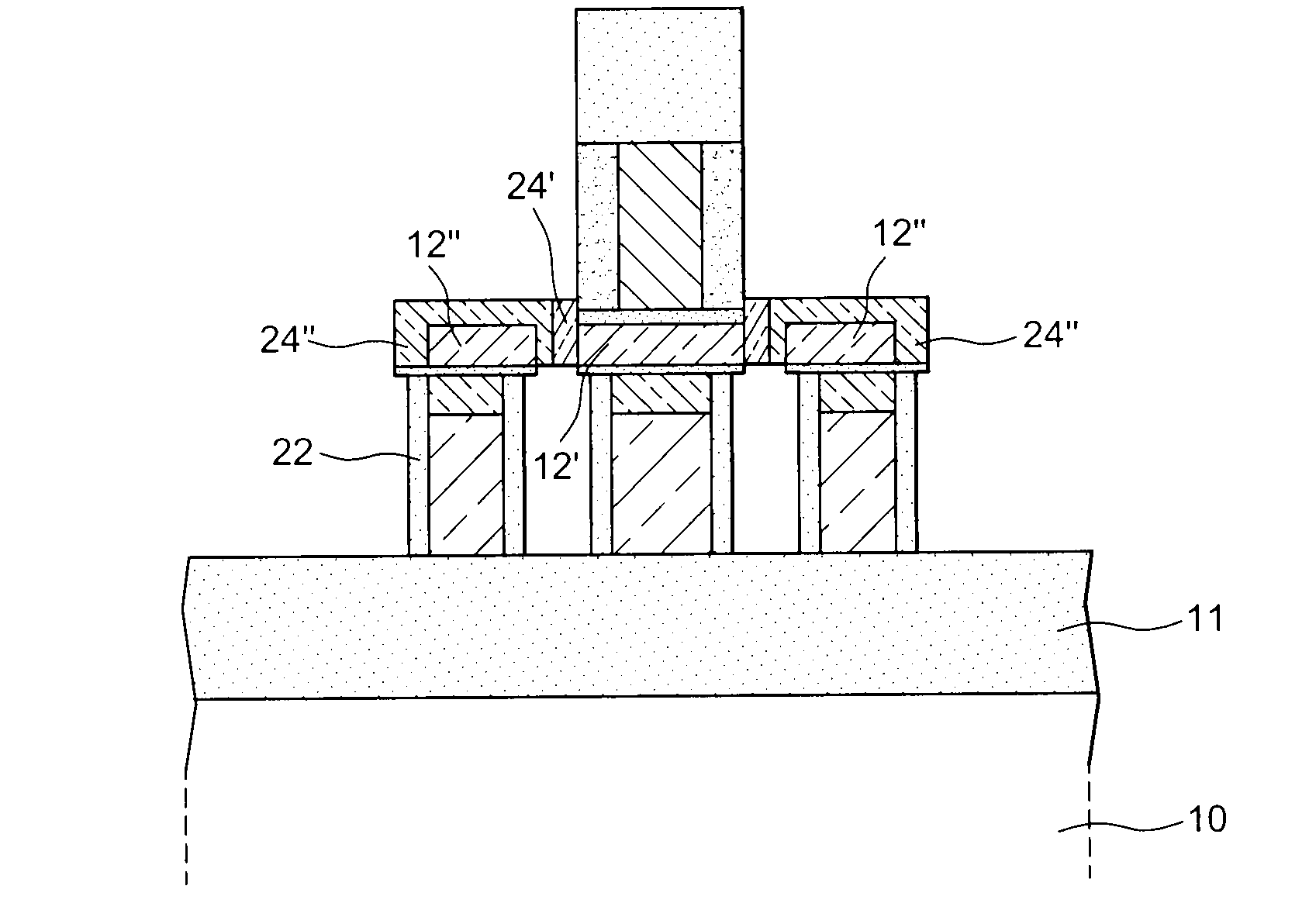
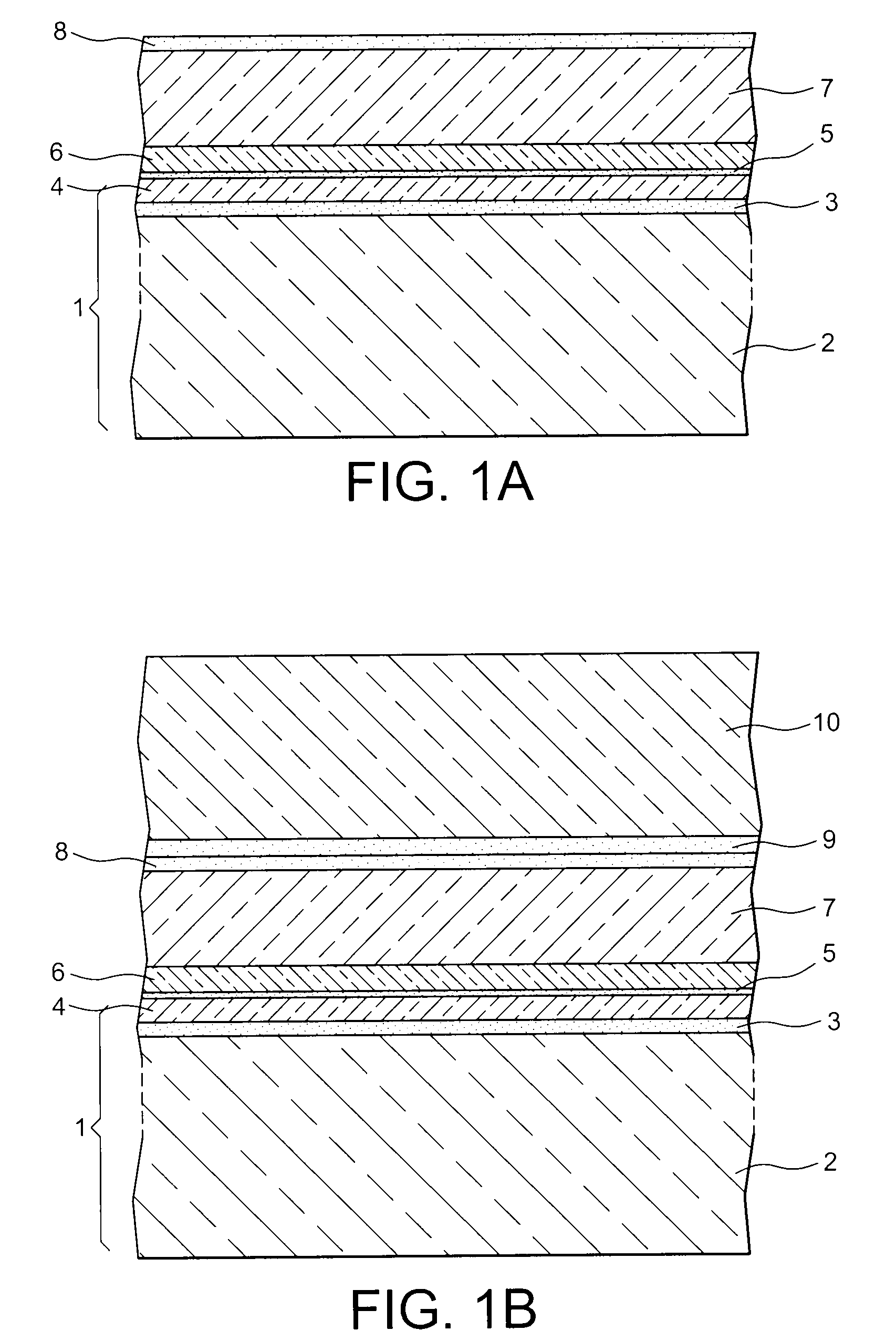
[0050]FIGS. 1A to 1E illustrate the preparatory steps of a method for manufacturing a field effect transistor with auto-aligned grids according to the invention. The method can then be continued according to a first variant illustrated by FIGS. 2A to 2J or according to a second variant illustrated by FIGS. 3A to 3I.

[0051]FIG. 1A shows a semiconductor substrate of the semiconductor-on-isolator type 1, for example a substrate SOI comprising a silicon support 2 supporting a layer 3 of silicon oxide and a layer 4 of silicon. This substrate could also be chosen from SSOI (Stressed Silicon on Isolator) and GeOI substrates, with an isolator which can be SiO2 or silicon nitride. On the layer 4 of silicon is deposited successively an isolating layer 5, a first layer 6 of rear grid material, a second layer 7 of rear grid material and a bonding layer 8, for example in silicon oxide.

[0052]If the layer 4 is in silicon, the isolating layer 5 is advantageously in silicon oxide. It provides the rea...


PUM


Abstract

The method comprises steps consisting of:forming, on an isolating face of a first substrate, a stack comprising successively at least one layer of rear grid material, an electrically insulating rear grid layer, a semi-conducting zone, an electrically insulating layer for the front grid, at least one layer of front grid material and a masking element, placed facing the semi-conducting zone,forming in the layer of front grid material a pattern reproducing the shape of the masking element and comprising etching of the layer of front grid material to eliminate the front grid material outside said pattern,forming on the free faces of the pattern a sacrificial spacer covering a first part of the semi-conducting zone revealed by eliminating the grid material,forming a protective layer over the remaining part, or second part, of the semi-conducting zone revealed by eliminating the grid material,eliminating the sacrificial spacer covering said first part of the semi-conducting zone,etching the first part of the semi-conducting zone revealed in the preceding step to delineate the channel of the transistor.

Description

TECHNICAL FIELD[0001]The invention relates to a method for manufacturing a field effect transistor with double grids, the grids being auto-aligned and horizontal.STATE OF THE PRIOR ART[0002]The document FR-A-2 829 294 (corresponding to U.S. Pat. No. 7,022,562) discloses a field effect transistor with horizontal auto-aligned grids and its method of manufacture. This transistor comprises an active region forming a channel, a first isolated grid associated with a first side of the active region, source and drain regions shaped in a part of the active region, on the other side of the channel and auto-aligned on the first grid, a second isolated grid associated with a second side of the active region, opposite the first side of the active region.[0003]The method for producing this transistor comprises the following steps:[0004]formation of a stack of layers comprising, starting from a supporting substrate: a first grid layer, a grid isolating layer, an active layer, a second grid isolati...

Claims


Application Information

Patent Timeline
IPC IPC(8): H01L21/84
CPCH01L21/28123H01L29/0847H01L29/66484H01L29/6653H01L29/78648H01L29/66636H01L29/66772H01L29/7831H01L29/78618H01L29/66628
Inventor PREVITALI, BERNARD
Owner COMMISSARIAT A LENERGIE ATOMIQUE ET AUX ENERGIES ALTERNATIVES
Why Eureka
Try Eureka