Diamond-like carbon electronic devices and methods of manufacture
- Summary
- Abstract
- Description
- Claims
- Application Information
AI Technical Summary
Benefits of technology
Problems solved by technology
Method used
Image

Examples
example 1
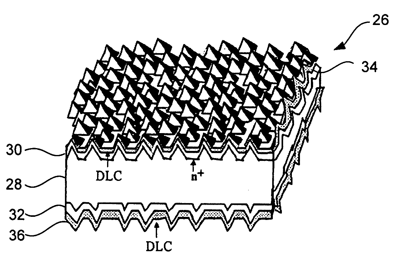
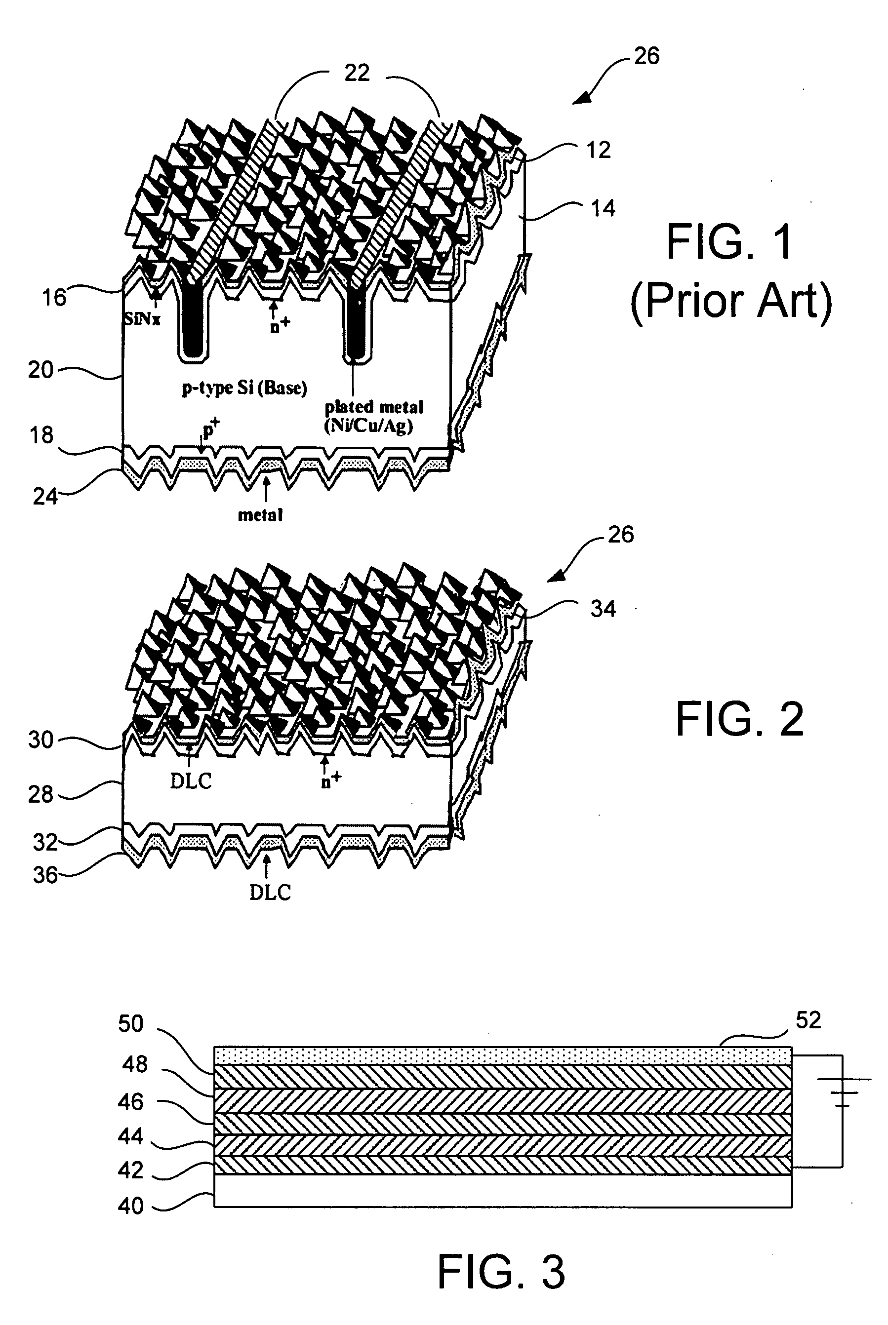
[0080]FIG. 3 illustrates a graded solar cell in accordance with the present invention. A chemical vapor deposition silicon film 40 of about 10 μm having micron grains serves as the photoelectric substrate. The silicon film is coated successively with silicon-carbon layers via chemical vapor deposition. Layers 42, 44, 46, 48 and 50 have a Si:C ratio of 10:90, 20:80, 30:70, 40:60 and 50:50 (SiC), respectively. Each layer is doped such that the graded portion represents a single p-n junction. A conductive diamond-like carbon film 52 having a thickness of about 10 μm is deposited on the SiC layer 50. The diamond-like carbon is deposited at partial vacuum of acetylene gas and 13.6 MHz to form the conductive diamond-like carbon which is also light transmissive. The resulting solar cell has layers having bandgaps from 1.1 eV for silicon to 3.3 eV for silicon carbide which covers most visible light, e.g. red about 1 eV while blue is about 3 eV.
PUM
 Abstract
Description
Claims
Application Information
 - R&D
- Intellectual Property
- Life Sciences
- Materials
- Tech Scout
- Unparalleled Data Quality
- Higher Quality Content
- 60% Fewer Hallucinations
Browse by: Latest US Patents, China's latest patents, Technical Efficacy Thesaurus, Application Domain, Technology Topic, Popular Technical Reports.
© 2025 PatSnap. All rights reserved.Legal|Privacy policy|Modern Slavery Act Transparency Statement|Sitemap|About US| Contact US: help@patsnap.com