Apparatus and method for measuring structures on a mask and or for calculating structures in a photoresist resulting from the structures
a technology of structures and masks, applied in the field of apparatus for measuring structures on masks and calculating structures in photoresists on wafers, can solve the problems of different results of measuring devices, measurement and measuring devices are not suitable for determining
- Summary
- Abstract
- Description
- Claims
- Application Information
AI Technical Summary
Benefits of technology
Problems solved by technology
Method used
Image
Examples
first embodiment
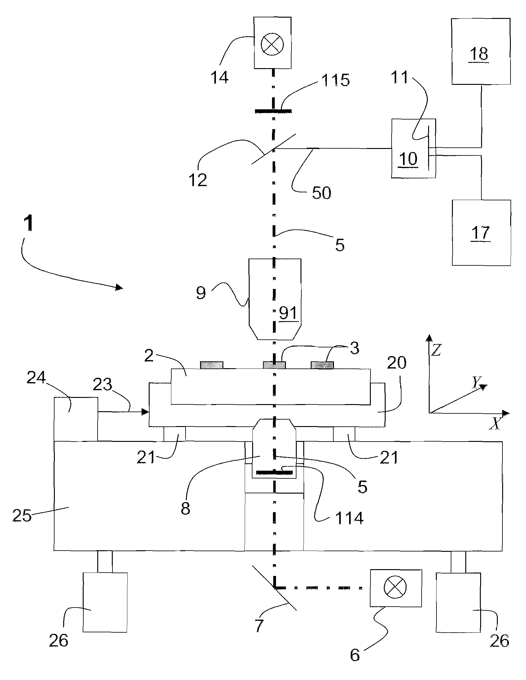
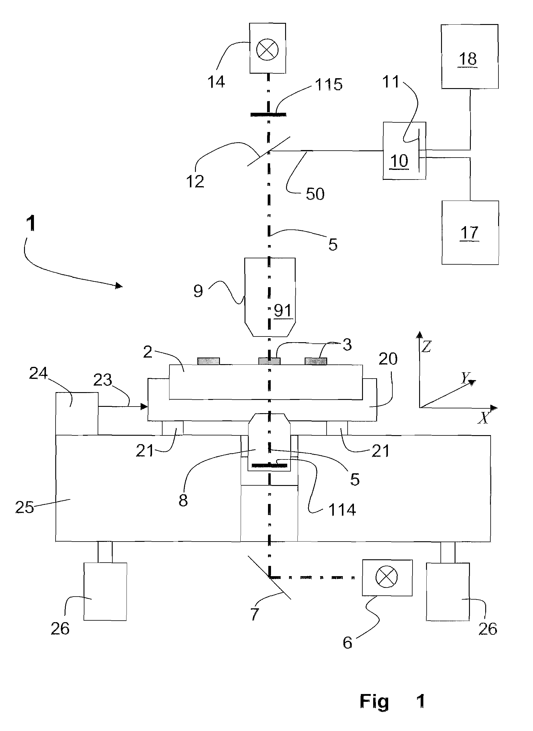
[0044]FIG. 1 is a schematic view of apparatus 1 according to the present invention, which is a coordinate measurement machine, as it has been known for some time from the prior art for measuring structures 3 on masks and / or wafers. The exemplary embodiment shown in FIG. 1 of apparatus 1 allows substrates to be optically inspected and measured. The substrate according to the present invention is a mask 2, for example of quartz glass. Mask 2 is used for the manufacturing of semiconductors, such as wafers. A plurality of structures 3 are applied to mask 2, which can be measured with the aid of apparatus 1. Apparatus 1 comprises an optical axis 5. A transmitted-light illumination means 6 is provided for the transmitted-light mode, which emits light in the near UV or DUV and passes the light via a mirror 7 towards a condenser 8. The light in optical axis 5 passes through substrate 2 and is at least substantially collected by an imaging optics 9 having a lens 91 and imaged onto a detector...
second embodiment
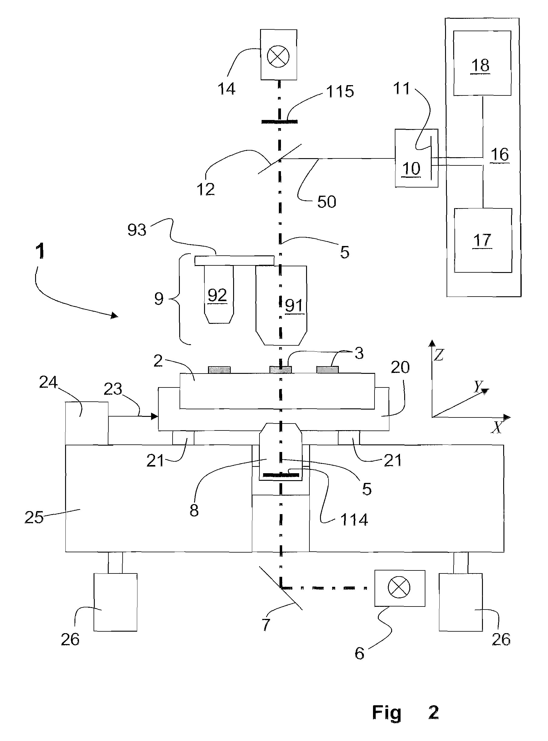
[0051]FIG. 2 shows the invention configured according to FIG. 1. In addition to lens 91, imaging optics 9 of apparatus 1 comprises at least one further lens 92. The at least two lenses 91, 92 are arranged on a slide 93 in the embodiment shown in FIG. 2. Depending on each wavelength used, this is how a suitable lens 91 or 92 can be brought into the beam path of optical axis 5 of apparatus 1. If the position and / or the CD of the structures on a mask 2 are to be determined, a wavelength in the near UV range or light of the wavelength of equal to or smaller than 400 nm is used, which is larger than the wavelength used in the stepper. If the printed pattern is to be evaluated, i.e. the structure to be expected in the photoresist on the wafer is to be calculated, lens 91 or 92 formed for the wavelength to be used in a stepper, is brought into the beam path of the apparatus.
PUM
 Abstract
Description
Claims
Application Information
 - R&D
- Intellectual Property
- Life Sciences
- Materials
- Tech Scout
- Unparalleled Data Quality
- Higher Quality Content
- 60% Fewer Hallucinations
Browse by: Latest US Patents, China's latest patents, Technical Efficacy Thesaurus, Application Domain, Technology Topic, Popular Technical Reports.
© 2025 PatSnap. All rights reserved.Legal|Privacy policy|Modern Slavery Act Transparency Statement|Sitemap|About US| Contact US: help@patsnap.com


