
Printed-Wiring Board, Bending Processing Method for Printed-Wiring Board, and Electronic Equipment

a technology of printed wiring and processing method, applied in the field of printed wiring board, can solve the problems of high water absorption of polyimide-based materials, many manufacturing problems, and high cost of polyimide-based materials

Inactive Publication Date: 2008-07-31
KK TOSHIBA
View PDF0 Cites 32 Cited by
  • Summary
  • Abstract
  • Description
  • Claims
  • Application Information

AI Technical Summary

Problems solved by technology

However, the polyimide-based material is high in water absorption and therefore subject to variations in shape and electrical characteristic due to moisture absorption.
In addition, the polyimide-based material is expensive.
Therefore, the use of the polyimide-based material causes many manufacturing problems.
In this case, however, the surface of the peeled-off portion may have irregularities and stress at the time of bending will be concentrated in the thin portion, causing the bending portion of the wiring board to be damaged.
Furthermore, this type of printed-wiring board has confirmed that cracks tends to develop in the bending portion at the boundary between the bending and rigid portions when a torsional stress is applied to the bending portion, for example, in a manufacturing step in which the wiring board is handled.

Method used


Image

  • Printed-Wiring Board, Bending Processing Method for Printed-Wiring Board, and Electronic Equipment
  • Printed-Wiring Board, Bending Processing Method for Printed-Wiring Board, and Electronic Equipment
  • Printed-Wiring Board, Bending Processing Method for Printed-Wiring Board, and Electronic Equipment

Examples


Embodiment Construction

[0024]Various embodiments according to the invention will be described hereinafter with reference to the accompanying drawings.

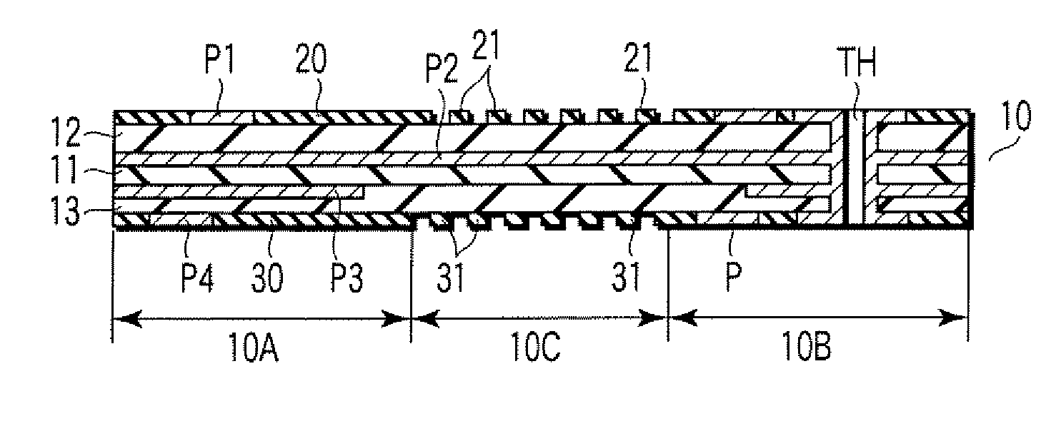
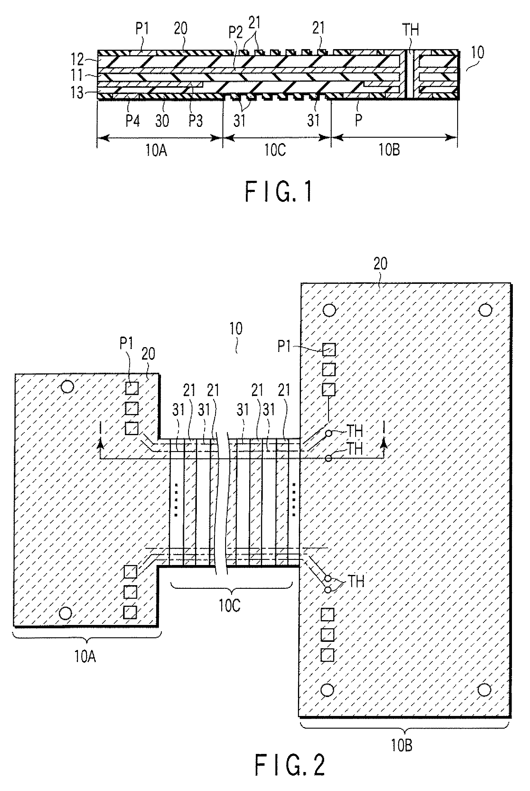
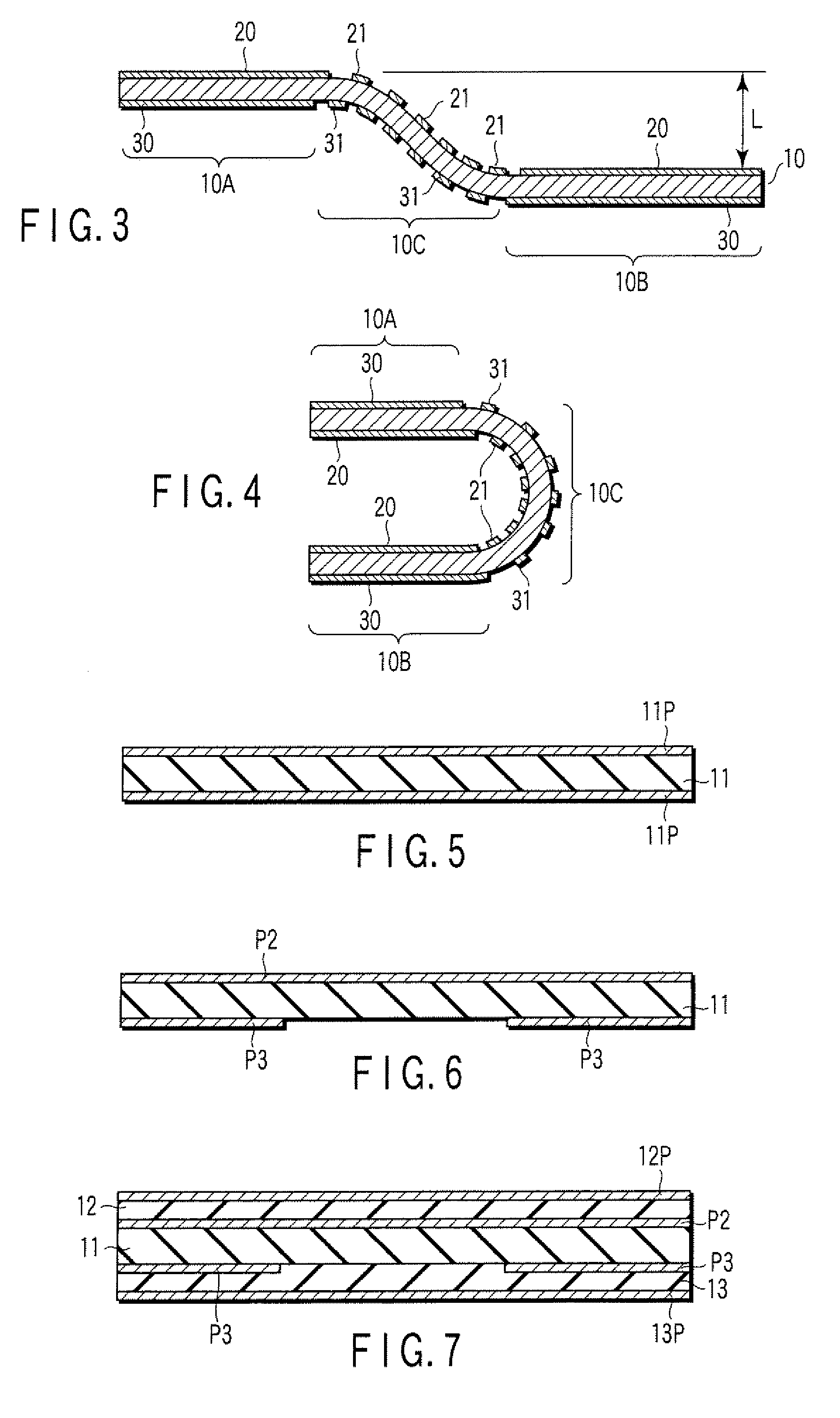
[0025]An embodiment of the present invention will be described hereinafter with reference to the accompanying drawings. A configuration of the printed-wiring board according to the embodiment of the invention is shown in FIGS. 1 and 2. This printed-wiring board shown in FIGS. 1 and 2 takes, as an example, a structure such that three layers of insulating material are stacked to form a composite or laminated board with four wiring layers so that the printed-wiring board is configured to have two rigid portions 10A, 10B and a bending portion 10C interposed between the rigid portions 10A and 10B.

[0026]The printed-wiring board of the embodiment is configured, as shown in FIG. 1, such that a composite or laminated board 10, which is formed with four wiring layers P1, P2, P3 and P4 each formed of a copper or aluminum film and three flexible layers 11, 12 and 13 eac...


PUM

PropertyMeasurementUnit
Electrical resistanceaaaaaaaaaa
Flexibilityaaaaaaaaaa
Electrical conductoraaaaaaaaaa

Abstract

According to one embodiment, there is provided a printed-wiring board in which a composite board is formed to have rigid portions and a bending portion, wherein the bending portion includes linear protrusions each formed with solder resist having a bending resistance property.

Description

CROSS-REFERENCE TO RELATED APPLICATIONS[0001]This application is based upon and claims the benefit of priority from Japanese Patent Application No. 2006-294619, filed Oct. 30, 2006, the entire contents of which are incorporated herein by reference.BACKGROUND[0002]1. Field[0003]One embodiment of the present invention relates to a printed-wiring board in which rigid board portions and a bending portion are formed in a laminated board.[0004]2. Description of the Related Art[0005]A technique that allows a portion of a rigid printed-wiring board to have a bending property is one which forms a bending portion between rigid boards by interposing an insulating layer made of a flexible insulating material between the rigid boards and integrating the rigid boards with the insulating layer interposed therebetween. This technique is implemented by using a polyimide-based insulating material, which is used as an FPC base material, as the flexible insulating material.[0006]However, the polyimide-...

Claims


Application Information

Patent Timeline
IPC IPC(8): H05K1/03H05K3/00
CPCH05K1/028H05K3/28Y10T29/49117H05K2201/0989H05K2201/09909H05K3/3452
Inventor ISHII, NORIHIROTAMAI, SADAHIROKANO, TERUNARI
Owner KK TOSHIBA
Learn More