
Semiconductor apparatus and buffer control circuit

Inactive Publication Date: 2008-07-03
FUJITSU SEMICON LTD
View PDF10 Cites 5 Cited by
  • Summary
  • Abstract
  • Description
  • Claims
  • Application Information

AI Technical Summary

Benefits of technology

[0014]According to the above aspect of the present invention, it is possible to start burst-transferring of the data stored in the buffer to the data storage unit before full amount of data to be transferred in a single burst-transfer is stored in the buffer, leading to an improved throughput of data transfer.
[0015]According to an embodiment, the buffer control unit may allow the burst-transfer of the data stored in the buffer to be started so as to prevent any location in the buffer in which no data to be burst-transferred has been stored from being read.
[0021]a register for storing a predetermined amount value determined such that the buffer control circuit allows burst-transfer of data stored in the buffer to be started before full amount of data to be transferred in a single burst-transfer is stored in the buffer so as to prevent any location in the buffer in which no data to be burst-transferred has been stored from being read; and
[0025]allowing the buffer to start burst-transfer of the data stored therein before full amount of data to be transferred in a single burst-transfer is stored in the buffer, so as to prevent any location in the buffer in which no data to be burst-transferred has been stored from being read.

Problems solved by technology

As a result, the control method is only applicable to such a situation in which the burst output of data from the frame memory starts periodically.

Method used


Image

  • Semiconductor apparatus and buffer control circuit
  • Semiconductor apparatus and buffer control circuit
  • Semiconductor apparatus and buffer control circuit

Examples


Embodiment Construction

[0039]The preferred embodiments of the present invention are described below with reference to the drawings.

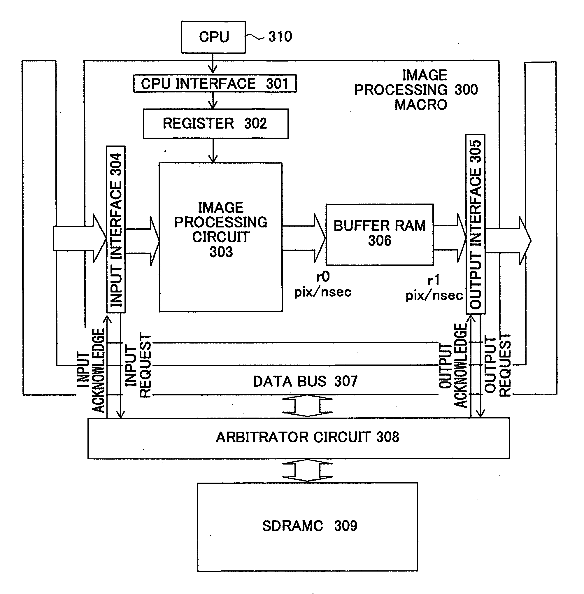
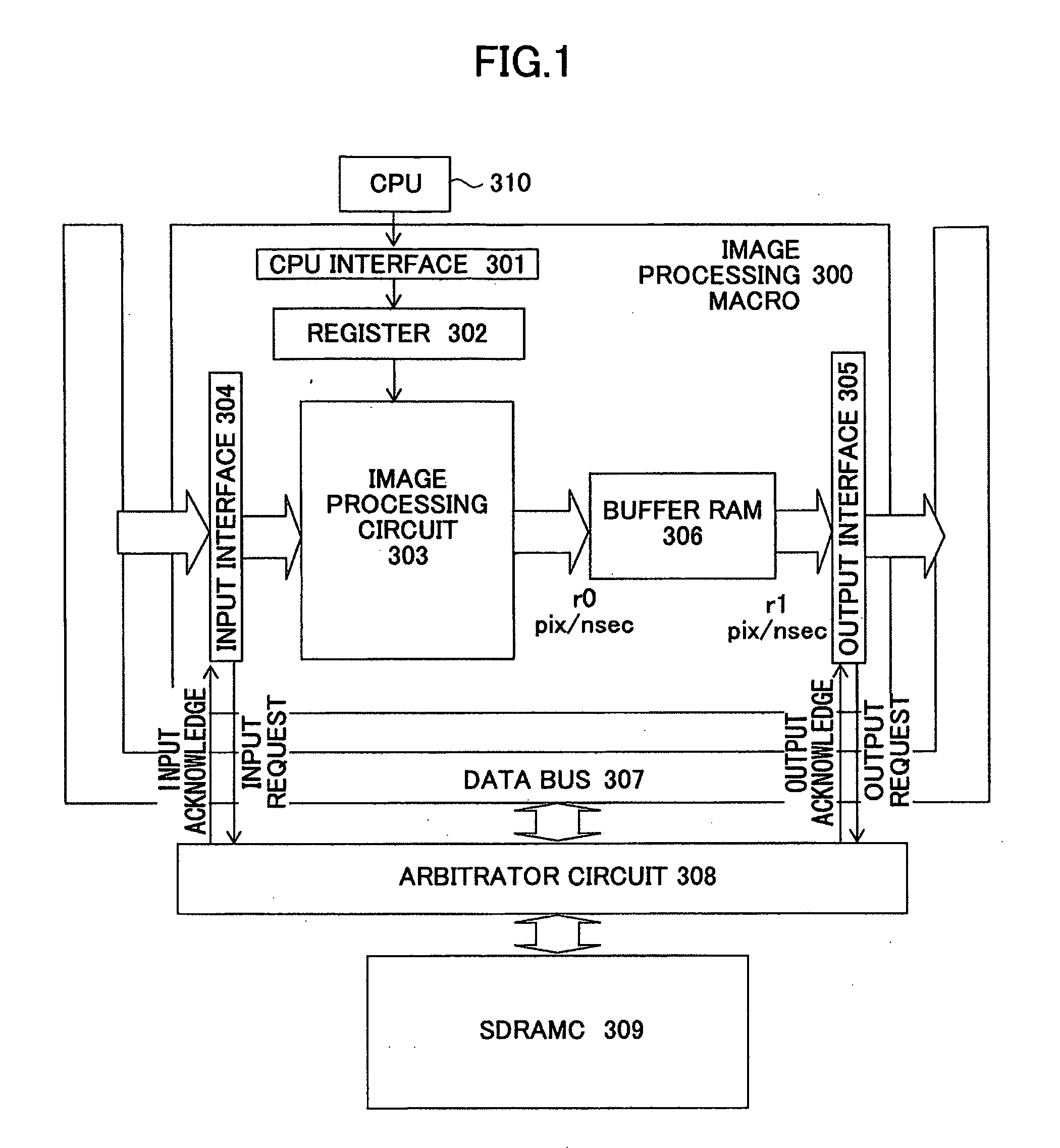
[0040]FIG. 1 is a block diagram showing an image processing macro for processing images. The image processing macro may be a part of a semiconductor integrated circuit (IC or LSI, for example) for processing image data. The semiconductor integrated circuit may be built in image capturing devices such as digital cameras and cell phones with image capturing function.

[0041]As shown in the figure, the image processing macro 300 may include a CPU (central processing unit) interface301, a register 302, an image processing circuit 303, an input interface 304, an output interface 305, and a buffer RAM (random access memory) 306. The CPU interface 301 is an interface circuit for interfacing the image processing macro 300 with a CPU (central processing unit) for controlling the image processing macro 300. The CPU is provided outside of the image processing macro 300 and connected theret...


PUM


Abstract

A semiconductor apparatus comprises a data processing unit for processing data, a buffer for temporarily storing the data processed by the data processing unit, and a buffer control unit for causing the data stored in the buffer to be burst-transferred to a data storage unit. The buffer control unit allows burst-transfer of the data stored in the buffer to be started before full amount of data to be transferred in a single burst-transfer is stored in the buffer.

Description

BACKGROUND OF THE INVENTION[0001]1. Field of the Invention[0002]The present invention generally relates to a semiconductor apparatus, and more particularly, to a semiconductor apparatus that temporality stores processed data in a buffer for subsequent burst transfer.[0003]2. Description of the Related Art[0004]A variety of data processing has been achieved by means of various integrated circuits. Video cameras and digital cameras, for example, have integrated circuits for processing in various manner image data captured with an image sensor. Cell phones and portable music players, for example, are equipped with integrated circuits for processing in various manner audio data stored therein. Such integrated circuits for processing a large amount of data, such as image data and audio data, are intensively developed for high throughput.[0005]JP 2006-267661, for example, describes an input signal processing part that makes the phenomenon that image information write to a memory and image...

Claims


Application Information

Patent Timeline
IPC IPC(8): G06F13/14
CPCG06F13/28G11C7/1057G11C7/22G11C11/4093G11C11/4096
Inventor OGURA, HIROKAZUMUTAGUCHI, KOHEI
Owner FUJITSU SEMICON LTD
Learn More