
Non-contact process kit

a process kit and non-contact technology, applied in the direction of electrolysis components, vacuum evaporation coatings, coatings, etc., can solve the problems of stressing materials, prone to flaking and particle generation, and the temperature of the cover ring may fluctuate during the process cycle, so as to minimize the effect of process contamination from films deposited thereon and excellent and predictable temperature control

Active Publication Date: 2008-06-19
APPLIED MATERIALS INC
View PDF7 Cites 71 Cited by
  • Summary
  • Abstract
  • Description
  • Claims
  • Application Information

AI Technical Summary

Benefits of technology

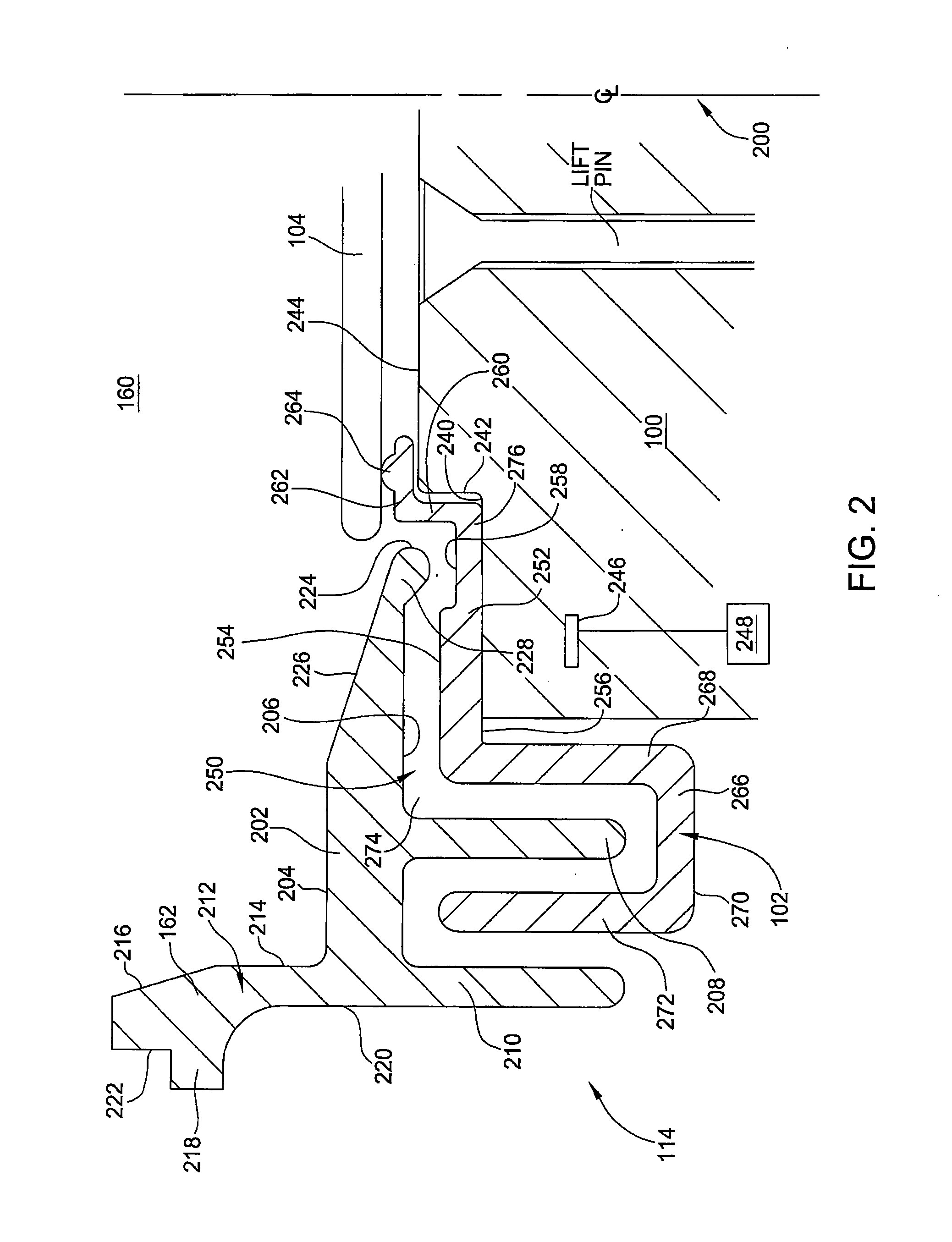
[0010]The invention generally provides a process kit for use in a physical vapor deposition (PVD) chamber, and a PVD chamber having an interleaving process kit. In one embodiment, a process kit includes an interleaving deposition ring and ground shield. The deposition ring is configured to have a large pedestal contact surface and a plurality of substrate supporting buttons. When installed in a PVD chamber, the interleaving deposition ring and ground shield advantageously are maintained in contact with the substrate support pedestal and chamber walls, thereby promoting excellent and predictable temperature control that substantially minimize process contamination from films deposited thereon. Moreover, the interleaving deposition ring and ground shield advantageously are configured not come into contact during use within the PVD chamber, thereby eliminating a potential source of particle generation present in conventional designs.

Problems solved by technology

As the rings and shield periodically contact each other as the substrate support pedestal raises and lowers between transfer and process positions, conventional designs are potential source of particulate contamination.
Moreover, since conventional cover ring designs are generally unconnected to temperature control sources, such as a chamber wall or substrate support pedestal, the temperature of the cover ring may fluctuate during the process cycle.
The heating and cooling of the cover ring increases the stress in materials deposited on the cover ring, making the stressed material prone to flaking and particle generation.

Method used


Image

  • Non-contact process kit
  • Non-contact process kit
  • Non-contact process kit

Examples


Embodiment Construction

[0022]The invention generally provides a process kit for use in a physical vapor deposition (PVD) chamber. The process kit advantageously has reduced potential for generating particulate contamination, which promotes greater process uniformity and repeatability along with longer chamber component service life.

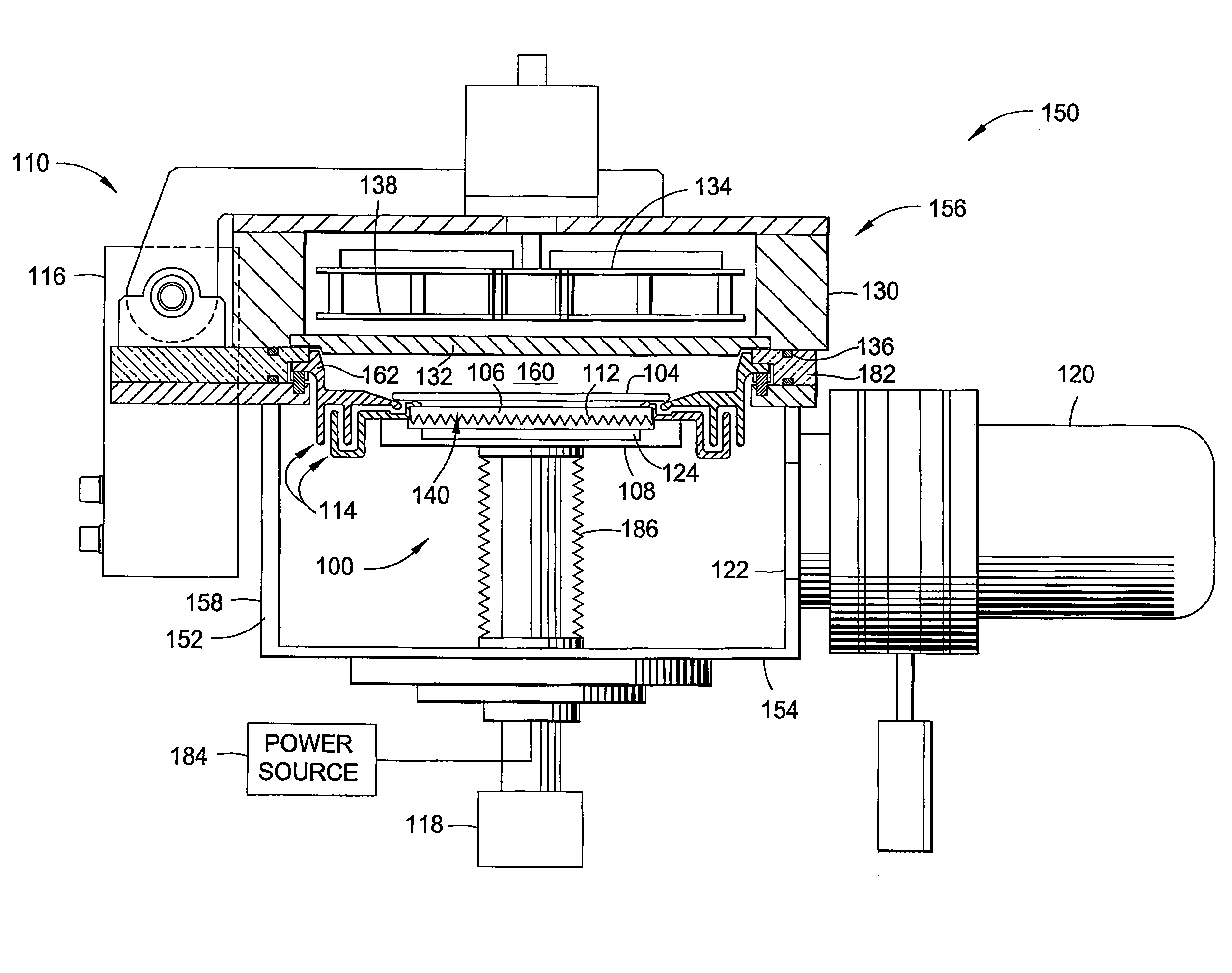
[0023]FIG. 1 depicts an exemplary semiconductor processing chamber 150 having one embodiment of a process kit 114. The process kit 114 includes an interleaving deposition ring 102 and ground shield 162. One example of a processing chamber that may be adapted to benefit from the invention is an IMP VECTRA™ PVD processing chamber, available from Applied Materials, Inc., of Santa Clara, Calif. It is contemplated that other processing chambers, including those from other manufacturers, may be adapted to benefit from the invention.

[0024]The exemplary processing chamber 150 includes a chamber body 152 having a bottom 154, lid assembly 156 and sidewalls 158 that define an evacuable in...


PUM

PropertyMeasurementUnit
Angleaaaaaaaaaa
Diameteraaaaaaaaaa
Electrical conductoraaaaaaaaaa

Abstract

A process kit for use in a physical vapor deposition (PVD) chamber, along with a PVD chamber having a non-contact process kit are provided. In one embodiment, a process kit includes a generally cylindrical shield that has a substantially flat cylindrical body, at least one elongated cylindrical ring extending downward from the body, and a mounting portion extending upwards from an upper surface of the body. In another embodiment, a process kit includes a generally cylindrical deposition ring. The deposition ring includes a substantially flat cylindrical body, at least one downwardly extending u-channel coupled to an outer portion of the body, an inner wall extending upward from an upper surface of an inner region of the body, and a substrate support ledge extending radially inward from the inner wall.

Description

CROSS REFERENCE TO RELATED APPLICATIONS[0001]This application claims benefit of U.S. Provisional Patent Application No. 60 / 870,752, filed Dec. 19, 2006 (APPM / 11725L) and to U.S. Provisional Patent Application No. 60 / 916,784, filed May 8, 2007 (APPM / 11725L02), both of which are incorporated herein by reference in their entireties.BACKGROUND OF THE INVENTION[0002]1. Field of the Invention[0003]Embodiments of the invention generally relate to a process kit for a semiconductor processing chamber, and a semiconductor processing chamber having a process kit. More specifically, the invention relates to a process kit that includes a ring and shield suitable for use in a physical vapor deposition chamber.[0004]2. Description of the Related Art[0005]Physical vapor deposition (PVD), or sputtering, is one of the most commonly used processes in the fabrication of electronic devices. PVD is a plasma process performed in a vacuum chamber where a negatively biased target is exposed to a plasma of a...

Claims


Application Information

Patent Timeline
IPC IPC(8): C23C14/30
CPCC23C14/564H01L21/68735H01L21/67069
Inventor BROWN, KARLBAJAJ, PUNEET
Owner APPLIED MATERIALS INC
Learn More