Liquid crystal display and display panel thereof

a liquid crystal display and display panel technology, applied in the direction of instruments, static indicating devices, etc., can solve the problems of image flickering of tft-lcd, increase in flicker noise of display panel, so-called rc delay

Active Publication Date: 2008-05-22
CHUNGHWA PICTURE TUBES LTD
View PDF3 Cites 26 Cited by
  • Summary
  • Abstract
  • Description
  • Claims
  • Application Information

AI Technical Summary

Benefits of technology

[0018]Accordingly, the present invention provides a display panel, in which a common voltage generation circuit is electrically connected to at least a pixel in a non-active pixel region, and a common voltage of the pixel corresponding to one column of pixels in the display panel is automatically adjusted in N frame time (N is a positive integer, e.g. 2). Thereby, the complicated process of conventional manual adjustment of the common voltage can be eliminated. Furthermore, the common voltage supplied is ensured to be at a best voltage level required by the column of the pixels in the display panel.
[0019]The present invention further provides a display to which the spirit of said display panel can be applied. Thereby, not only can the advantages of the display panel disclosed in the present invention be achieved, but the flicker noises of the display panel can be minimized, thus leading to an improvement of the display quality.
[0037]In the display and the display panel thereof provided by the present invention, the common voltage generation circuit is electrically connected to at least one second pixel in the second pixel region i.e. the non-active pixel region in the display panel, and obtains an average of the voltages having positive and negative polarities in N frame time (N is a positive integer e.g. 2.) according to the display voltage of the drain of the TFT in the second pixel. Then, the average is utilized as the common voltage and provided to each of the first pixels in the first pixel region i.e. the active pixel region in the display panel. Thereby, the complicated process of conventional manual adjustment of the common voltage can be eliminated. Furthermore, the common voltage supplied is ensured to be at the best voltage level required by the column of the pixels in the display panel.
[0038]In addition, given that the common voltage generation circuit is electrically connected to more than two second pixels in the second pixel region i.e. the non-active pixel region, the problem of the drift of the feed-through voltage (ΔVD) caused by an RC delay of the parasitic capacitance and the parasitic resistance on the scan line can be avoided. Thereby, the gray-level accuracy of each of the first pixels in the first pixel region in the display panel can be significantly improved, and the flicker noises of the display panel can be reduced, thus promoting the display quality.

Problems solved by technology

Accordingly, said ΔVGP is affected by the parasitic capacitance and the parasitic resistance on the scan line, thus resulting in a so-called RC delay.
As described above, both factors resulting in different feed-through voltages (ΔVD) of the scan voltages lead to an increase in flicker noises of the display panel, and thereby images displayed by the TFT-LCD flicker.
Moreover, each display panel has different characteristics, and therefore said best common voltage Vcom and the fine-tuned corrected gamma voltage outside the source driver may not be applicable to all display panels.
However, if a technology of driving a multi-level e.g. a three- or a four-level scan voltage is intended to be developed according to said solution 2, it is obvious that said development complicates the design of the gate driver.
Besides, given that the voltage level Vp cannot be accurately calculated by the gate driver, the feed-through voltage ΔVD of the scan voltage VG of the scan line Gm may be insufficiently or excessively compensated, which results in uncertainties in terms of design and measurement.

Method used


Image

  • Liquid crystal display and display panel thereof
  • Liquid crystal display and display panel thereof
  • Liquid crystal display and display panel thereof

Examples


Embodiment Construction

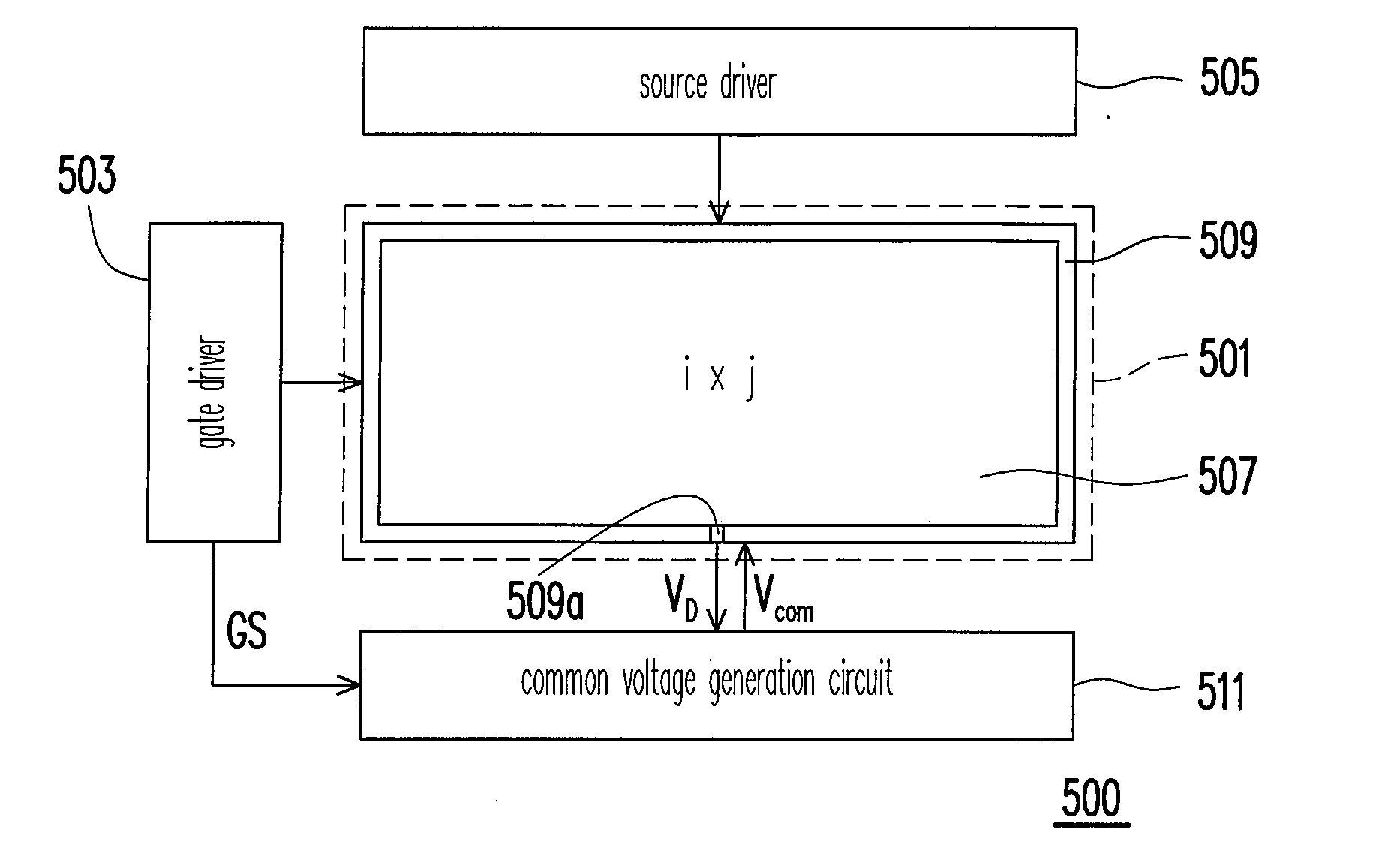
[0049]FIG. 5 is a block diagram depicting a display 500 according to one embodiment of the present invention. Please refer to FIG. 5. The display 500 e.g. an LCD includes a display panel 501 e.g. an LCD panel, a gate driver 503, and a source driver 505. In the present embodiment, the display panel 501 includes a first pixel region 507, a second pixel region 509, and a common voltage generation circuit 511. The first pixel region 507 has a plurality of first pixels (not shown) arranged in an i*j array for displaying images. Here, i and j are positive integers. The second pixel region 509 has a plurality of second pixels 509a disposed in the periphery of the first pixel region 507.

[0050]The common voltage generation circuit 511 is electrically connected to one of the second pixels 509a in the second pixel region 509, and the second pixel 509a corresponds to one column of the pixels in the first pixel region 507. In addition, the common voltage generation circuit 511 provides a common ...


PUM


Abstract

An LCD and a display panel thereof are provided. A common voltage generation circuit of the display panel is electrically connected to at least one pixel in a non-active pixels region. According to the display voltage at a drain of a TFT in the pixel, an average of display voltages of positive and negative polarities is obtained in two frame times. The average value is regarded as a common voltage supplied to every pixel in an active pixel region in the display panel. Thereby, the problem of a drift of a feed-through voltage (ΔVD) of a scan voltage due to an RC delay of a parasitic-capacitance and a parasitic-resistance on the scan line can be avoided. Further, the gray-level accuracy of every pixel in the active pixel region can be improved, and the flicker-noise of the display-panel can be reduced, thus significantly promoting the display quality of the LCD.

Description

CROSS-REFERENCE TO RELATED APPLICATION[0001]This application claims the priority benefit of Taiwan application serial no. 95142533, filed Nov. 17, 2006. All disclosure of the Taiwan application is incorporated herein by reference.BACKGROUND OF THE INVENTION[0002]1. Field of the Invention[0003]The present invention relates to a display and a display panel thereof, and more particularly to a liquid crystal display and a display panel thereof capable of adjusting a common voltage automatically.[0004]2. Description of Related Art[0005]In recent years, liquid crystal displays (LCDS) have been widely adopted and have replaced the conventional cathode ray tube (CRT) displays. Currently, the LCDs have become one of the mainstream products in the market of displays. With the progress of the semiconductor technology, LCD panels have the advantages of low power consumption, slimness and compactness, high resolution, high color saturation, long life time, and so on. Therefore, the LCD panels ha...

Claims


Application Information

Patent Timeline
IPC IPC(8): G09G3/36
CPCG09G3/3696G09G2320/0223G09G2320/0219G09G2300/0852G09G3/3655G09G2320/0247G09G2310/0232G09G3/3666
Inventor TU, CHANG-CHING
Owner CHUNGHWA PICTURE TUBES LTD
Why Eureka
Try Eureka