
Properties In Electronic Design Automation

a technology of electronic design and automation, applied in the field of electronic design automation, can solve the problem that devices cannot be manually designed, and achieve the effect of efficient data processing

Active Publication Date: 2008-05-15
SIEMENS PROD LIFECYCLE MANAGEMENT SOFTWARE INC
View PDF9 Cites 17 Cited by
  • Summary
  • Abstract
  • Description
  • Claims
  • Application Information

AI Technical Summary

Benefits of technology

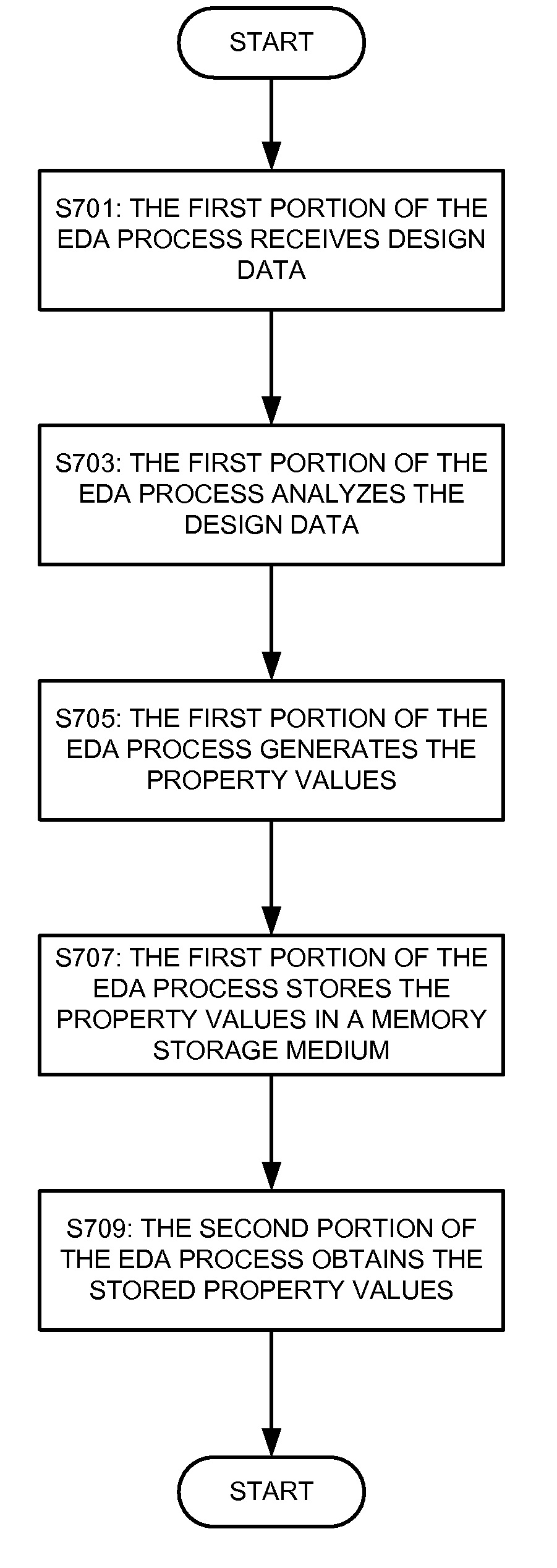
[0011]Advantageously, various implementations of the invention may allow a first electronic design automation process to generate one or more property values. The generated property values can then be passed to another electronic design automation process. For example, a design rule check (DRC) process may generate one or more property values for each of a plurality of geometric elements in a physical layout design. The design rule check process can then pass these property values onto a second electronic design automation process, such as an optical proximity correction (OPC) process. By using the property values provided by the design rule check process, the optical proximity correction process can avoid having to recalculate the property values. This use of property values may be particularly beneficial where the second electronic design automation process cannot easily calculate the property values itself, or where the second electronic design automation process cannot calculate the property values as quickly or efficiently as the first electronic design automation process.

Problems solved by technology

Many microdevices, such as integrated circuits, have become so complex that these devices cannot be manually designed.
In addition, however, the design rule check process also may determine the likelihood that the polygons may nonetheless form the wiring lines with an erroneous bridging fault.

Method used


Image

  • Properties In Electronic Design Automation
  • Properties In Electronic Design Automation
  • Properties In Electronic Design Automation

Examples


Embodiment Construction

Exemplary Operating Environment

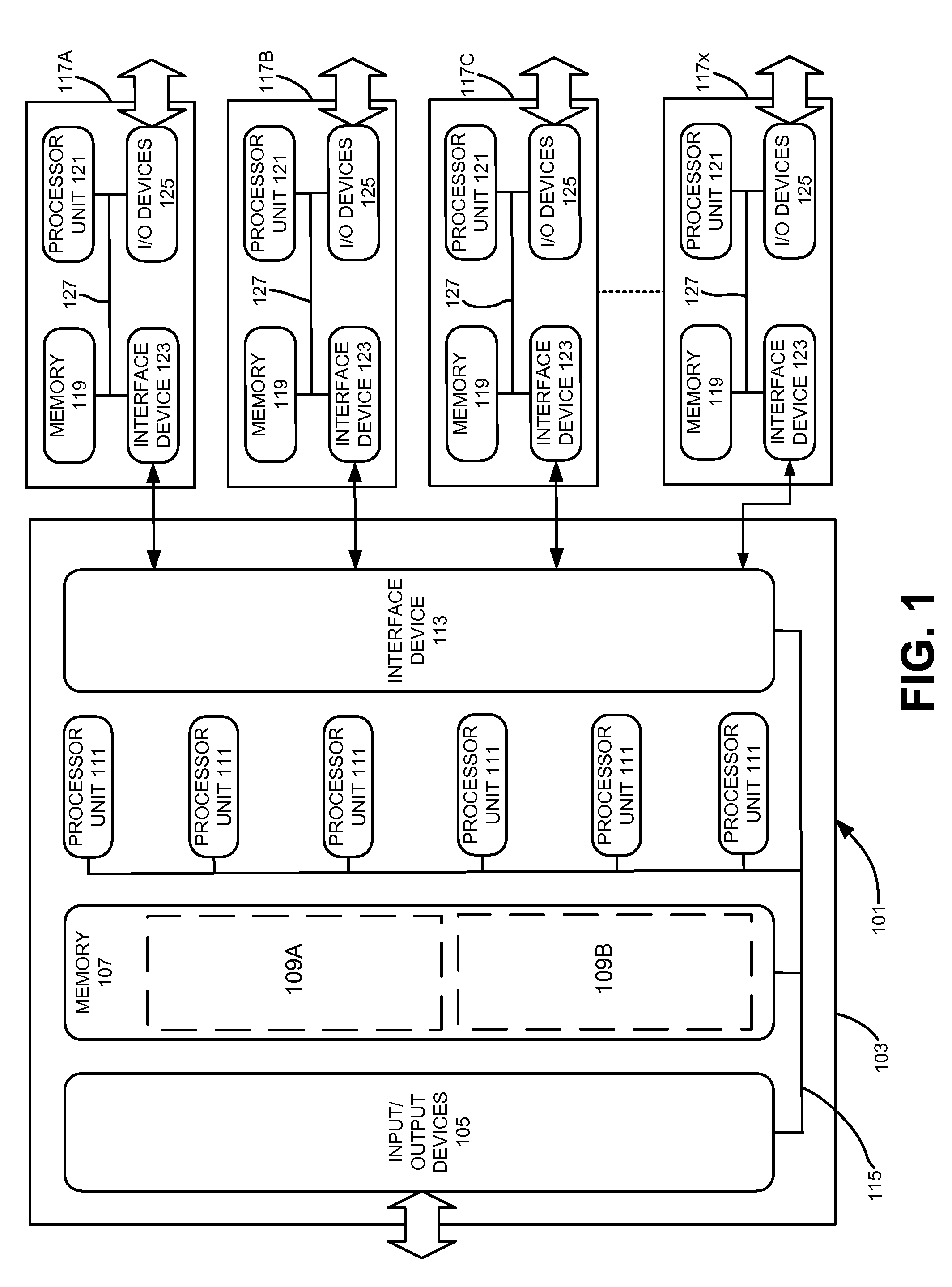
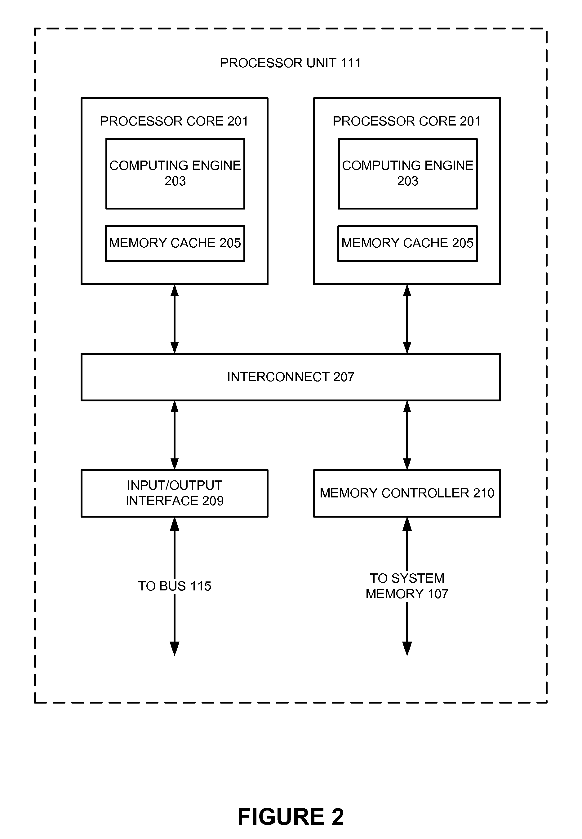
[0021]The execution of various electronic design automation processes according to embodiments of the invention may be implemented using computer-executable software instructions executed by one or more programmable computing devices. Because these embodiments of the invention may be implemented using software instructions, the components and operation of a generic programmable computer system on which various embodiments of the invention may be employed will first be described. Further, because of the complexity of some electronic design automation processes and the large size of many circuit designs, various electronic design automation tools are configured to operate on a computing system capable of simultaneously running multiple processing threads. The components and operation of a computer network having a host or master computer and one or more remote or servant computers therefore will be described with reference to FIG. 1. This operating envir...


PUM


Abstract

One or more properties can be associated with a design object in a microdevice design. The design object may be an object in a physical layout design for a microdevice, such as a geometric element in a layout design. The design object also may be a collection of geometric elements in a layout design, such as a net, a cell in a hierarchical design, or even a collection of all of the geometric elements in a layer of a design. Still further, the design object may even be an item in a logical circuit design, such as a net in a logical circuit design for an integrated circuit. The values of one or more properties may be statically assigned for or dynamically generated during a design process performed by an electronic design automation tool. A property may be assigned a constant value or a value defined by an equation or other type of script that includes one or more variables. A property may be simple, where the definition of the property's value is not dependent upon the value of any other properties. Alternately, a property may be a compound property, where the definition of the property's value incorporates another, previously-determined property value. Still further, a property may be an alternative property, where the property is assigned one value definition under a first set of conditions and assigned another value definition under a second set of conditions. A first electronic design automation process may generate one or more property values. The generated property values then can be passed to another electronic design automation process in the design analysis flow for its use.

Description

RELATED APPLICATIONS[0001]This application claims priority to U.S. Provisional Patent Application No. 60 / 850,716 entitled “Properties In Electronic Design Automation,” filed on Oct. 9, 2006, and naming Fedor Pikus as inventor, which application is incorporated entirely herein by reference.FIELD OF THE INVENTION[0002]The present invention is directed to the use of properties in electronic design automation. Various implementations of the invention may be useful for exchanging one or more properties between processes in an automated electronic design tool.BACKGROUND OF THE INVENTION[0003]Many microdevices, such as integrated circuits, have become so complex that these devices cannot be manually designed. For example, even a simple microprocessor may have millions and millions of transistors that cooperate to form the components of the microprocessor. As a result, electronic design automation tools have been created to assist circuit designers in analyzing a circuit design before it is...

Claims


Application Information

Patent Timeline
Patent Type & Authority Applications(United States)
IPC IPC(8): G06F17/50
CPCG06F2217/12G06F17/5081G06F30/398G06F2119/18Y02P90/02
Inventor PIKUS, FEDOR G.BROOKS, PHILLIP A.MYRON, GARY S.
Owner SIEMENS PROD LIFECYCLE MANAGEMENT SOFTWARE INC
Learn More