
Electro optic device, method of manufacturing electro optic device, and scanning type optical apparatus

a scanning type optical apparatus and electro optic technology, applied in non-linear optics, instruments, optics, etc., can solve the problems of limiting the use of polygon mirrors or galvano mirrors, complicated configuration and control of scanning systems, and the inability of scanning type image display apparatuses to have fixed pixels, etc., to achieve the effect of reducing power consumption and large deflection angl

Inactive Publication Date: 2008-05-15
SEIKO EPSON CORP
View PDF4 Cites 4 Cited by
  • Summary
  • Abstract
  • Description
  • Claims
  • Application Information

AI Technical Summary

Benefits of technology

[0013]An advantage of some aspects of the invention is that it provides an electro optic device capable of obtaining a large deflection angle and reducing power consumption, a method of manufacturing the electro optic device, and a scanning type optical apparatus.

Problems solved by technology

Moreover, the scanning type image display apparatus does not have fixed pixels unlike a liquid crystal display, a plasma display, and the like.
In this case, however, there is a problem that the configuration and control of a scanning system become complicated.
However, even though the apparatus using the polygon mirror is disclosed in JP-A-01-245780, there is a limit to the polygon mirror or the galvano mirror since the scanning frequency rises as an image format requests a high resolution.
As a result, it becomes complicated to control a signal.
In the case of such EO scanner, however, the following problems are still left.
However, in terms of the structure of the EO scanner, the distance between electrodes affects an optical path of scanned light.
Accordingly, if the distance is set to be too narrow, a laser beam propagating through the EO scanner touches the electrode, which causes a problem that light is not emitted from an emission end surface of EO crystal.
Moreover, even if the light is emitted from the emission end surface of EO crystal, it is not possible to obtain a large deflection angle in the EO crystal in which the distance between electrodes is narrow, that is, in the EO crystal having a small thickness.
That is, due to the structural problem described above, it is difficult to realize the improvement in efficiency of electric field intensity and an increase in deflection angle at the same time.
That is, if optical elements in which the distance between electrodes of the first and second electrodes increases in a stepwise manner are integrally formed, a fragment is generated and waste of crystal occurs.

Method used


Image

  • Electro optic device, method of manufacturing electro optic device, and scanning type optical apparatus
  • Electro optic device, method of manufacturing electro optic device, and scanning type optical apparatus
  • Electro optic device, method of manufacturing electro optic device, and scanning type optical apparatus

Examples


first embodiment

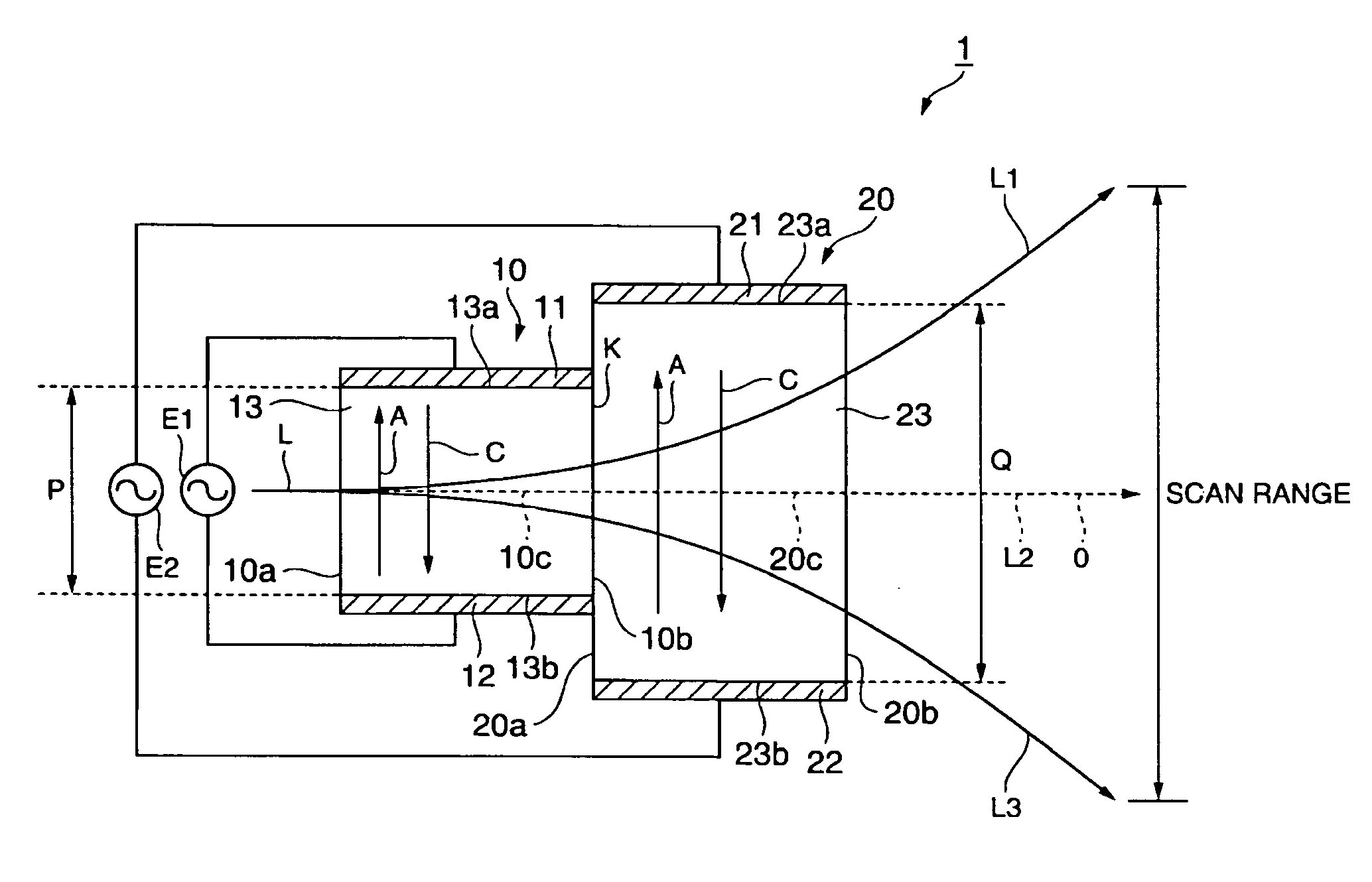
[0043]In an electro optic device 1, the refractive index distribution changes according to the intensity of an electric field generated therein, such that a laser beam propagating therethrough is scanned. Specifically, the electro optic device 1 includes a first electro optic element 10, which has an incident end surface 10a on which a laser beam is incident, and a second electro optic element 20, which has an emission end surface 20b from which a laser beam is emitted, as shown in FIG. 1. The first electro optic element 10 and the second electro optic element 20 are disposed such that an emission end surface 10b of the first electro optic element 10 and an incident end surface 20a of the second electro optic element 20 are in contact with each other in a state where central axes 10c and 20c of the first and second electro optic elements 10 and 20 match each other.

[0044]Moreover, configurations of the first and second electro optic elements 10 and 20 are equal to each other, but siz...

second embodiment

[0080]Next, a second embodiment of the invention will be described with reference to FIG. 6. In addition, in each embodiment to be described below, components common to those in the electro optic device 1 according to the first embodiment are denoted by the same reference numerals, and the description thereof will be omitted.

[0081]An electro optic device 40 according to the present embodiment is different from the electro optic device 1 according to the first embodiment from the view point of a voltage applied to the first electrode 11 and the second electrode 21.

[0082]First, as shown in FIG. 6, a plane that is perpendicular to an interface K between the first electro optic element 10 and the second electro optic element 20 and includes an intersection between the interface K and a central axis O1 of a laser beam L passing through the interface K, is assumed to be ‘M’.

[0083]In addition, a voltage that allows a refractive index of the optical element 13 and a refractive index of the ...

third embodiment

[0087]Next, a third embodiment of the invention will be described with reference to FIG. 7.

[0088]In the present embodiment, an image display apparatus (scanning type optical apparatus) 50 including the electro optic device 1 according to the first embodiment as a scanning unit will be described.

[0089]As shown in FIG. 7, an image display apparatus 50 includes: a red-colored light source (light source) 50R that emits a red-colored laser beam; a green-colored, light source (light source) 50G that emits a green-colored laser beam; a blue-colored light source (light source) 50B that emits a blue-colored laser beam; a cross dichroic prism 51; an electro optic device 1 that scans a laser beam emitted from the cross dichroic prism 51 in a horizontal direction of a screen 55; a galvano mirror 52 that causes the laser beam emitted from the electro optic device 1 to be scanned in a direction vertical to the screen 55; and the screen (projected surface) 55 onto which the laser beam scanned from...


PUM

PropertyMeasurementUnit
voltageaaaaaaaaaa
voltageaaaaaaaaaa
voltageaaaaaaaaaa

Abstract

An electro optic device includes an optical element in which a refractive index distribution, changes according to the intensity of an electric field generated therein such that an incident laser beam is scanned. First and second electrodes are provided on two opposite surfaces of the optical element. A distance between electrodes of the first and second electrodes of the optical element decreases continuously or in a stepwise manner from an emission end surface toward an incident end surface.

Description

BACKGROUND[0001]1 Technical Field[0002]The present invention relates to an electro optic device, a method of manufacturing an electro optic device, and a scanning type optical apparatus.[0003]2. Related Art[0004]In recent years, a scanning type image display apparatus that displays an image by raster scanning beam-shaped light, such as a laser beam, on a projected surface has been suggested. In such apparatus, completely black display may be realized by stopping supply of a laser beam. Accordingly, it becomes possible to realize a display having a higher contrast than, for example, a projector using a liquid crystal light valve. Moreover, the image display apparatus using a laser beam is characterized in that, for example, the color purity is high because the laser beam has a single wavelength and the laser beam is easily shaped (easily focused) because the laser beam has a high coherence. Accordingly, the image display apparatus using a laser beam is expected as a high-quality disp...

Claims


Application Information

Patent Timeline
Patent Type & Authority Applications(United States)
IPC IPC(8): G02F1/29
CPCG02F1/29G02F1/0322
Inventor NOJIMA, SHIGEO
Owner SEIKO EPSON CORP
Learn More