
Hexagonal Wurtzite Type Single Crystal, Process For Producing The Same, And Hexagonal Wurtzite Type Single Crystal Substrate

a technology of hexagonal wurtzite and single crystal, which is applied in the direction of crystal growth process, polycrystalline material growth, gel state, etc., can solve the problems of difficult to keep a stoichiometric mixture ratio, high pressure and high temperature condition of growth of crystal obtained thereby, and achieve excellent uniformity of impurity concentration and low impurity concentration. , the effect of low impurity concentration

Inactive Publication Date: 2008-03-06
MITSUBISHI CHEM CORP +1
View PDF1 Cites 50 Cited by
  • Summary
  • Abstract
  • Description
  • Claims
  • Application Information

AI Technical Summary

Benefits of technology

[0031] The single crystal with a hexagonal wurtzite structure can be used in a wide range of applications because it has a low impurity concentration and is excellent in uniformity of the impurity concentration. For example, a ZnO single crystal has a low impurity concentration and therefore has excellent transparency so that it can be used for optics application. In addition, since it is excellent in the uniformity of an impurity concentration, it is suited for use in dielectric devices and scintillators making use of the feature of it as a large-sized single crystal. In particular, in TOF PET (Time of Flight Positron Emission Tomography) which is expected to improve the detection accuracy of cancers by the tomographic observation of the whole body, a large-sized single crystal is used in the detector portion so that it is very important to equalize an impurity concentration in the crystal. The single crystal with a hexagonal wurtzite structure according to the present invention which features a small variation in the impurity concentration among c-plane substrates cut from the single crystal can be used without being influenced by the cutting site. Use of the m-plane or a-plane substrate is considerably useful because it reduces an in-plane variation in the impurity concentration, thereby enabling uniform detection properties.
[0032] The m-plane or a-plane substrate cut from the single crystal with a hexagonal wurtzite structure according to the present invention has a low impurity concentration, has almost no polarity and has excellent uniformity so that it is suited as a substrate for a device such as light emitting device (LED or t

Problems solved by technology

The gas phase methods and melt methods have the drawbacks that crystals obtained thereby have a high defect density and these methods require a very high pressure and high temperature condition for growth.
An electronegative element which is one of two elements constituting the crystal having a hexagonal wurtzite structure is a molecular gas of nitrogen or oxygen or an element having volatility such as sulfur or selenium and it is difficult to keep a stoichiometric mixture ratio of the composition with an electropositive element at the time of crystal growth.
It is however difficult to prevent generation of a defect, that is, loss of an electronegative element in the crystal, even under this environment.
Although a p type ZnO must be prepared for actualizing a light emitting device utilizing ZnO, ZnO easily generates defects such as oxygen deficiency and zinc in an interstitial site and tends to become not a p type but an n type.
This ZnO single crystal is not suited for an acoustoelectric effect device because of too high conductivity.
Even a ZnO single crystal which has grown in the presence of the above-described H2O2 is not suited as an acoustoelectric effect device because its conductivity is as low as 10−8˜10−10 1 / Ω·cm.
The ZnO single crystal has therefore improved conductivity by depositing Zn vapor onto the surface of the thus-obtained ZnO single crystal, thereby increasing the Zn concentration on the surface excessively.
The improvement of the conductivity by the Zn vapor deposition as described above is however accomplished only in the proximity of the surface of the ZnO single crystal obtained by the vapor deposition, and the ZnO single crystal still has a problem that the single crystal as a whole lacks uniformity in the conductivity.
In addition, such vapor deposition requires a large-scaled apparatus, which is disadvantageous from the standpoint of a manufacturing cost.

Method used


Image

  • Hexagonal Wurtzite Type Single Crystal, Process For Producing The Same, And Hexagonal Wurtzite Type Single Crystal Substrate
  • Hexagonal Wurtzite Type Single Crystal, Process For Producing The Same, And Hexagonal Wurtzite Type Single Crystal Substrate
  • Hexagonal Wurtzite Type Single Crystal, Process For Producing The Same, And Hexagonal Wurtzite Type Single Crystal Substrate

Examples


example 1

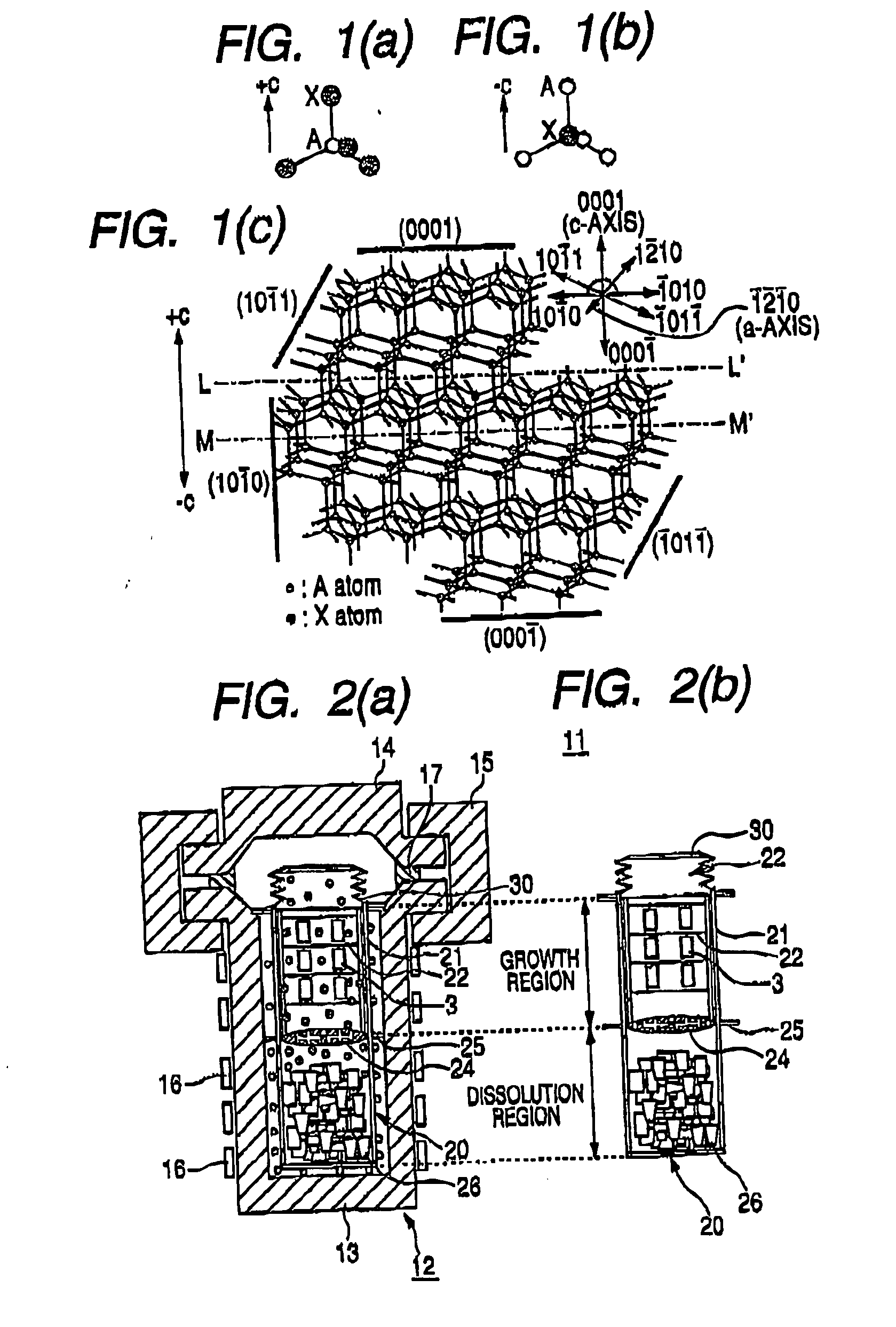
[0085] After ZnO powders having a purity of 99.9999% were compacted in a molding vessel and sintered at 1100° C. for 24 hours, the solid thus obtained was filled in the growth vessel 20. Purified water in which 1 mol / l of LiOH and 3 mol / l of KOH had been dissolved as a mineralizer was poured in 80% of the free capacity of the growth vessel 20 and then 0.05 mol / l of H2O2 was poured therein further. The growth vessel 20 and bellows were welded to completely seal the growth vessel 20. For the thermal conductivity between the autoclave 12 (φ200×300 mm) and the growth vessel 20, purified water was filled therein in an amount of 80% of the free capacity. The autoclave 12 comprising a vessel body 13 and a lid 14 was made airtight by placing the lid 14 on the vessel body 13 via a packing 17 and fixing them with a fixing member 15.

[0086] The dissolution region (having the same meaning as the raw material filling portion, which will equally apply hereinafter) and the growth region (having th...

example 2

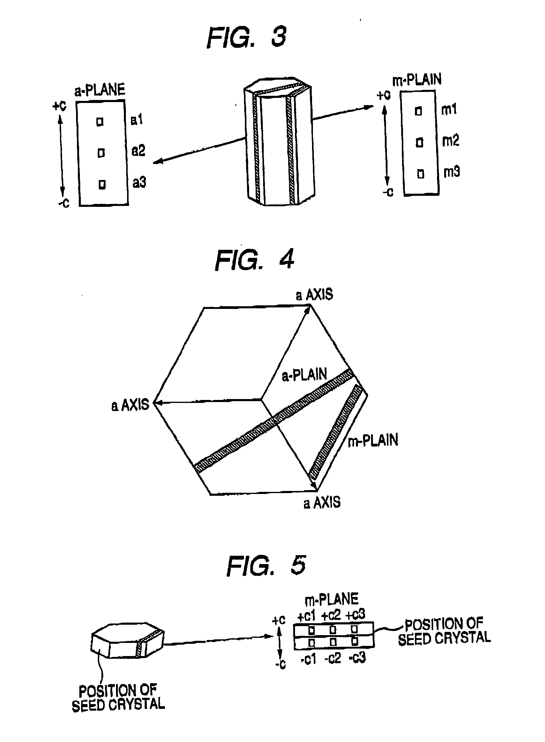
[0089] In a similar manner to Example 1 except that a final temperature difference between the raw material filling portion and crystal growth portion was set at 45° C., crystal growth of ZnO was performed. Described specifically, the temperature of the dissolution region was made greater by 35 to 45° C. than the temperature of the growth region and heating was conducted to give the final temperature of the dissolution region of 390° C. and that of the growth region of about 345° C. As a result, a crystal having a size of 60 mm (a)×10 mm (m)×20 mm (c) and having high transparency was obtained (in which, a, m and c represents the directions of respective axes). Analysis results of metal concentrations in regions N-1 to N-3 of the sample cut in FIG. 6 by a similar method to that employed in Example 1 are shown in Table 2. The results suggest that the concentration of Fe is 1.3 ppm or less, that of Al is 0.5 ppm or less and that of Mg is 0.1 ppm or less and a variation in the concentra...

example 3

[0090] In a similar manner to Example 1 except that a final temperature difference between the raw material filling portion and crystal growth portion was set at 17° C., crystal growth of ZnO was performed. Described specifically, the temperature of the dissolution region was made greater by from 10 to 20° C. than the temperature of the growth region and heating was conducted to give the final temperature of the dissolution region of 355° C. and that of the growth region of about 338° C. As a result, a crystal having a size of 28 mm (a)×11.5 mm (m)×14 mm (c) and colored in green was obtained (in which, a, m and c represents the directions of respective axes). Analysis results of metal concentrations in regions O-1 to O-4 of the sample cut as in FIG. 7 by a similar method to that employed in Example 1 are shown in Table 2. The results suggest that the variation in each metal concentration within the same plane was within 100%, but the sample contained Fe, Al and Mg in a relatively la...


PUM


Abstract

Provided is a single crystal with a hexagonal wurtzite structure which is useful as a substrate for various devices and has high purity and is uniform. The single crystal with a hexagonal wurtzite structures which is obtained by a crystal growth on at least an m-plane of a columnar seed crystal and represented by AX (A representing an electropositive element and X representing an electronegative element) is characterized in that a variation in the concentration of a metal other than the electropositive element A and having a concentration of 0.1 to 50 ppm is within 100%.

Description

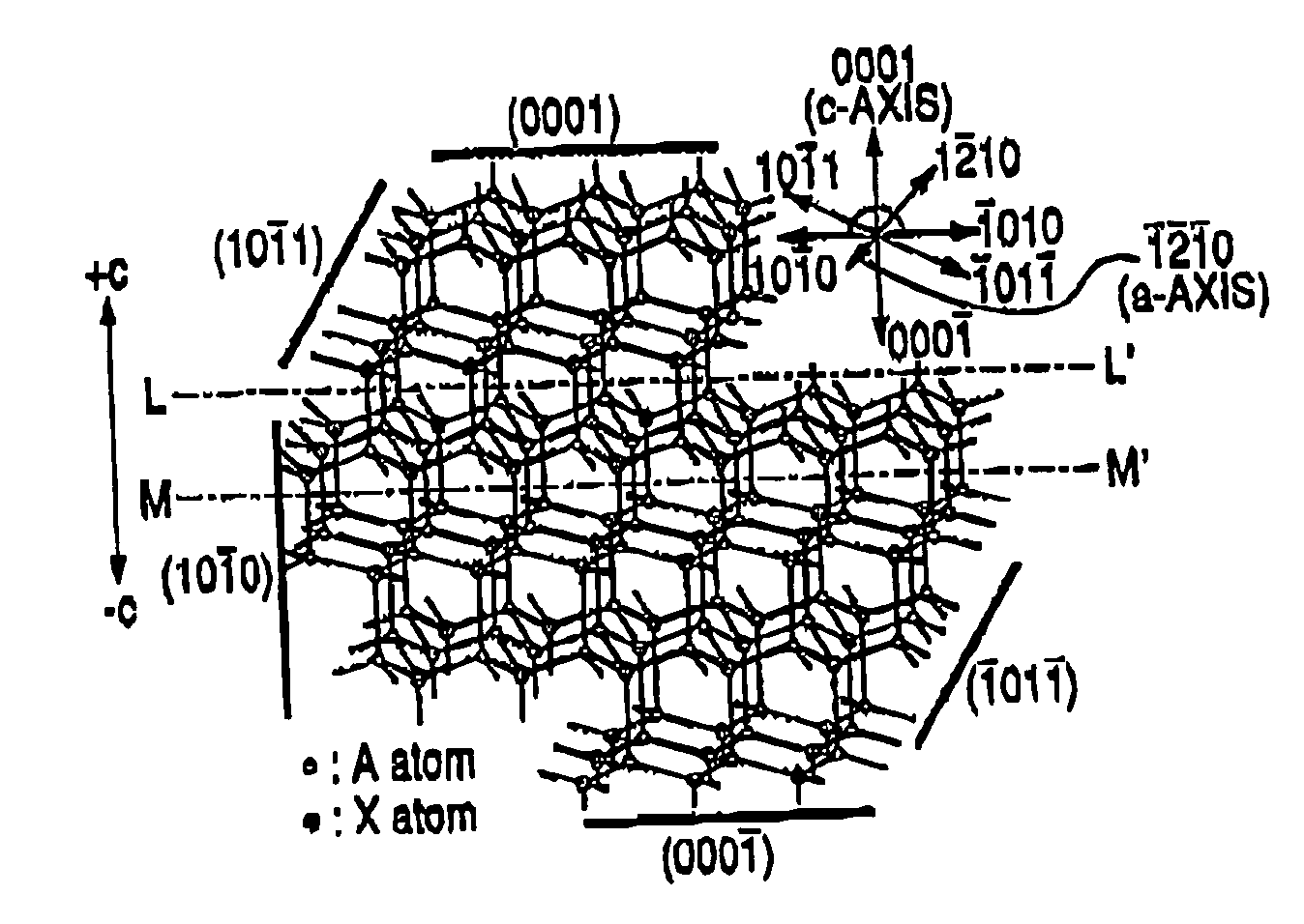
TECHNICAL FIELD [0001] The present invention relates to a single crystal with a hexagonal wurtzite structure, a production process thereof, and a single crystal substrate with a hexagonal wurtzite structure. [0002] Hexagonal crystals have three a axes which make an angle of 120° within a regular hexagonal plane and one c axis which is vertical thereto, totally four crystallographic axes. A plane vertical to the c axis is called “c plane”, a plane parallel to the c axis and any one of a-axes is “m plane”, and a plane parallel to the c axis and vertical to any one of the a axes is called “a plane”. Atomic arrangement of a crystal structure found in a compound represented by AX (wherein, A represents an electropositive element and X represents an electronegative element), that is, a wurtzite structure, among hexagonal crystal systems, is shown in FIG. 1. The A atom and X atom each has an arrangement close to the hexagonal close-packed structure. The A atom has four tetrahedrally-coordi...

Claims


Application Information

Patent Timeline
IPC IPC(8): C30B29/16C30B7/10
CPCC30B29/16C30B7/10
Inventor YOSHIOKA, KENJIYONEYAMA, HIROSHIMAEDA, KATSUMINIIKURA, IKUOSATO, MITSURUITO, MASUMIORITO, FUMIO
Owner MITSUBISHI CHEM CORP
Learn More