Liquid crystal display panel and method for manufacturing the same

a liquid crystal display and liquid crystal technology, applied in the field can solve the problems of difficulty in reducing the number of manufacturing facilities or reducing the cost of processing, affecting the quality of liquid crystal display panels, so as to reduce the number of photolithographic processes, reduce the number of processes, and improve the quality

Inactive Publication Date: 2008-03-06
FUTURE VISION
View PDF5 Cites 3 Cited by
  • Summary
  • Abstract
  • Description
  • Claims
  • Application Information

AI Technical Summary

Benefits of technology

[0030]It is an object of the present invention to provide a liquid crystal display panel and a method for manufacturing the same, by which it is possible to narrow down the gap between the source electrode and the drain electrode to 4 μm or less without increasing the number of processes by using the ink jet direct drawing on the electrodes and the lines on the thin-film transistor.
[0031]To attain the above object, in the liquid crystal display panel of the present invention, the source electrode and the drain electrode of the thin-film transistor are made up with conductive layers disposed at opposed positions with a first gap on upper layer of an active layer and a laminated layer of transparent conductive film disposed at opposed positions with a second gap, which is narrower than the first gap on each of the opposed ends of the conductive layers to cover the opposed ends of the conductive layer disposed at opposed positions respectively to the upper layer of said active layer. By this manufacturing method, it is possible to reduce the number of photolithographic processes for forming the thin-film transistor by using direct drawing of ink jet to form the conductive layers and to obtain very fine gap for narrower channel by laminating a transparent conductive film on it and by separating it through photolithographic process.
[0032]According to the present invention, it is possible to extensively reduce the number of processes required for the formation of the thin-film transistor to be used in the liquid crystal display panel and to manufacture a liquid crystal display panel with very fine quality at lower cost.

Problems solved by technology

However, it is difficult to reduce the number of the manufacturing facilities or to extensively reduce the cost of the processing by the repeating of such processes.
Even when the gap between the source electrode and the drain electrode is prepared by combination of the ink jet direct drawing method and the pattern etching, the photolithographic process is still required, and this causes an obstacle to the reduction of the cost.
Although the thin-film transistor can be prepared in easier manner by the adoption of ink jet direct drawing method, it is difficult in the patterning process by the ink jet direct drawing method to prepare a pattern with a narrow width of 30 μm or less.

Method used


Image

  • Liquid crystal display panel and method for manufacturing the same
  • Liquid crystal display panel and method for manufacturing the same
  • Liquid crystal display panel and method for manufacturing the same

Examples


Embodiment Construction

[0043]Detailed description will be given below on an embodiment of the invention referring to the attached drawings.

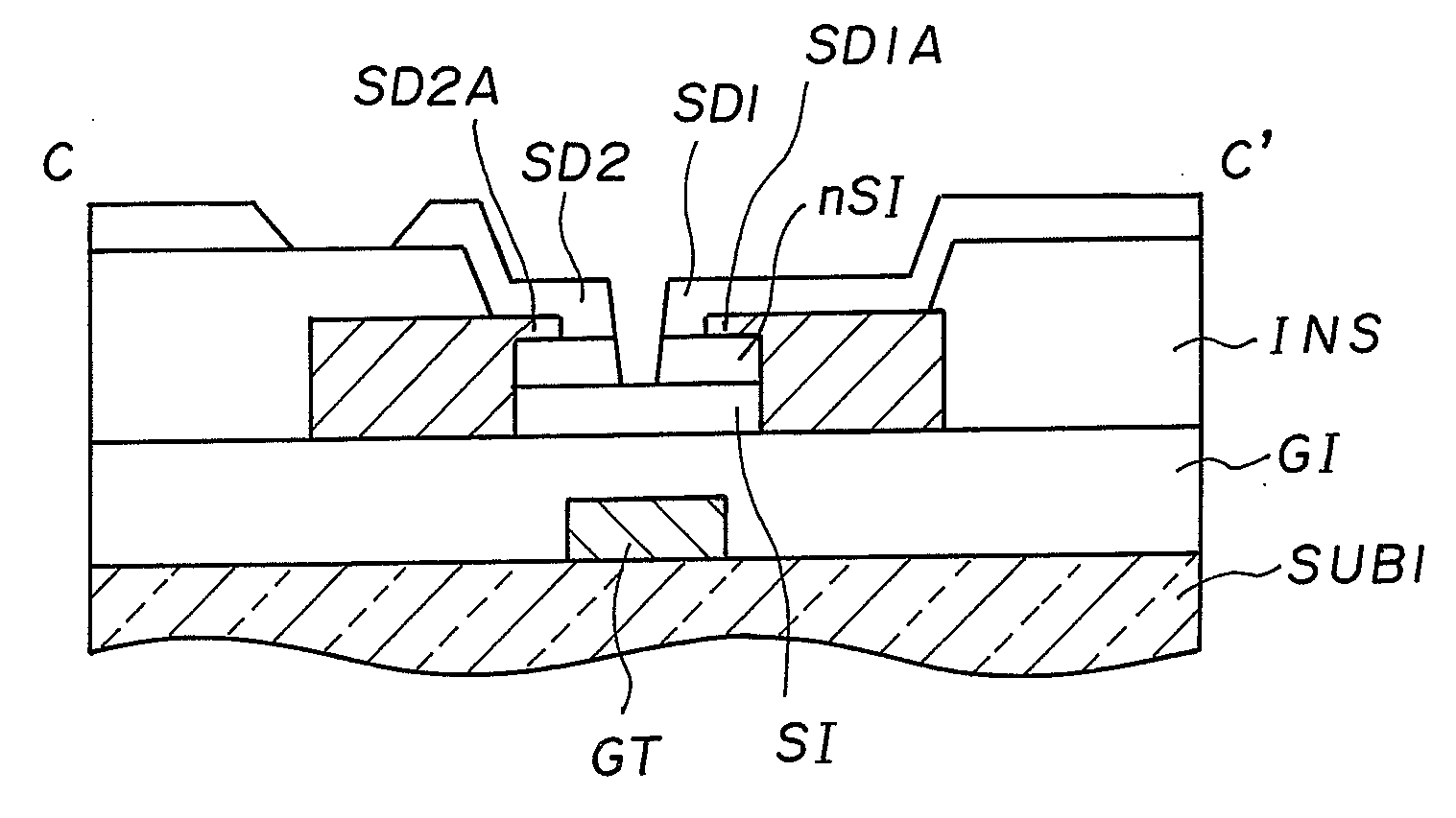
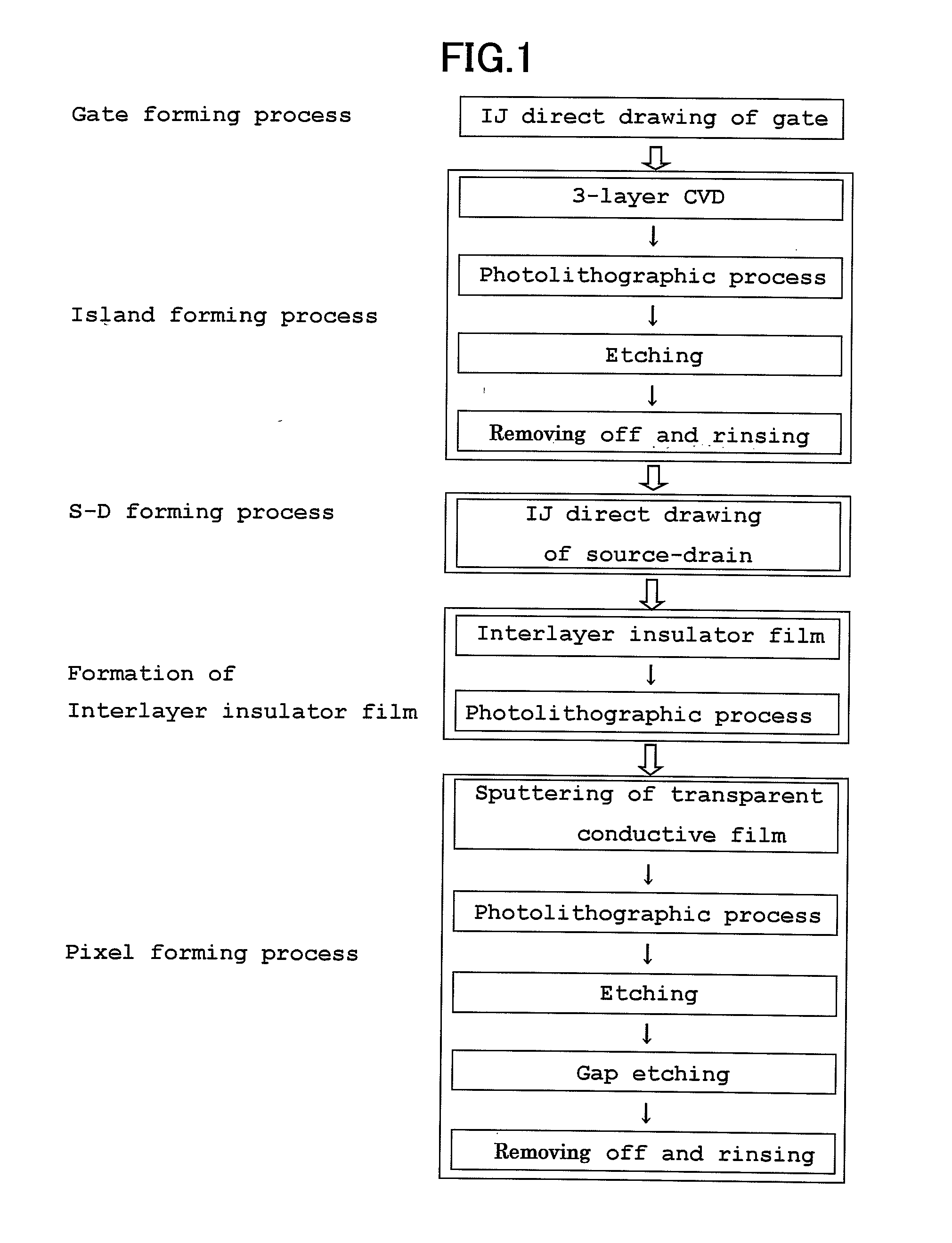
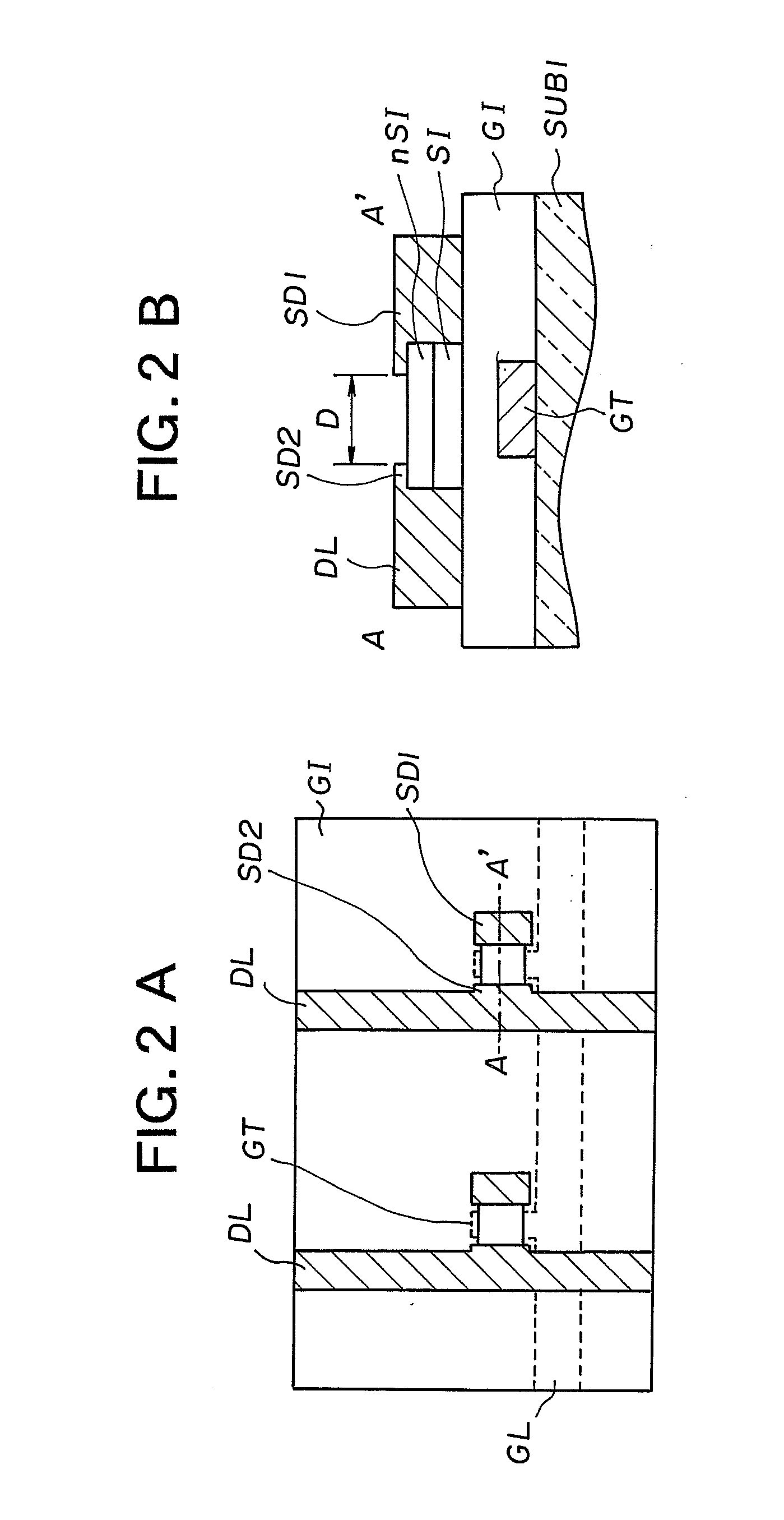
[0044]FIG. 1 is a process chart to explain an essential portion of a process for manufacturing a first substrate (a thin-film transistor substrate) to be used in a liquid crystal display panel of the present invention. First, a gate electrode and a gate line are prepared by direct drawing of ink jet on inner surface (above an underlying film) of a first substrate (thin-film transistor substrate), which is preferably made of a glass substrate. The direct drawing of the gate electrode and the gate line is the same as the gate direct drawing process as explained the lower portion of FIG. 10.

[0045]In the island forming process, after the formation of the gate, a gate insulator film, a silicon semiconductor layer, and an n+ silicon layer, which is to be turned to a contact layer, are deposited in this order by CVD method (3-layer CVD method). A photosensitive resist is coat...


PUM

PropertyMeasurementUnit
widthaaaaaaaaaa
widthaaaaaaaaaa
widthaaaaaaaaaa

Abstract

The present invention provides a new technique, in which direct drawing of ink jet is used and a gap between a source electrode and a drain electrode is narrowed down to 4 μm or less without increasing the number of processes. According to this technique, a conductive layer SD1A and a conductive layer SD2A arranged at opposed positions with a first gap are prepared by direct drawing of ink jet on upper layer of a silicon semiconductor layer SI by forming a source electrode SD1 and a drain electrode SD2 on a thin-film transistor, and by a laminating layer of the transparent conductive films SD1 and SD2 with a second gap, which is narrower than the first gap between the opposed ends of the conductive layers, to cover the upper layer of said first layer and the opposed ends of the conductive layers arranged at opposed positions.

Description

BACKGROUND OF THE INVENTION[0001]1. Field of the Invention[0002]The present invention relates to a liquid crystal display system. In particular, the invention relates to an active matrix type liquid crystal display panel and a method for manufacturing the same.[0003]2. Background of the Invention[0004]A liquid crystal display panel system of this type comprises a liquid crystal display panel PNL and a combination of a driving circuit and peripheral devices such as backlight. FIG. 8 is a schematical cross-sectional view to explain an example of approximate arrangement of a typical longitudinal electric field type (the so-called TN type) liquid crystal display system. Normally, a liquid crystal display panel, which makes up an active matrix type liquid crystal display system, is prepared by sealing a liquid crystal LC between a first panel PNL1 comprising a first substrate (an active matrix substrate or a thin-film transistor substrate) and a second substrate (a counter substrate or a...

Claims


Application Information

Patent Timeline
Patent Type & Authority Applications(United States)
IPC IPC(8): G02F1/1368H01L21/336
CPCG02F1/1368H01L27/1292H01L27/1288H01L27/124G02F1/136
Inventor YOSHIMOTO, YOSHIKAZU
Owner FUTURE VISION
Why Eureka
Try Eureka