
Memory Control Circuit, Nonvolatile Storage Apparatus, and Memory Control Method

a memory control circuit and non-volatile storage technology, applied in the direction of digital storage, error detection/correction, instruments, etc., can solve the problem of flash memory failing to write data, and achieve the effect of preventing an increase of bad blocks, reducing the frequency of error termination to write instruction from a host, and reducing the price of non-volatile memory

Inactive Publication Date: 2008-02-28
PANASONIC CORP
View PDF6 Cites 140 Cited by
  • Summary
  • Abstract
  • Description
  • Claims
  • Application Information

AI Technical Summary

Benefits of technology

[0020] The present invention can prevent an increase of bad blocks since written data is reread even if a nonvolatile memory easily occurring a writing error is used and a bad block processing is executed only when a predetermined number or more errors are occurred. In addition, frequency of error termination to writing instruction from a host can be reduced by executing retry of writing of correctable data to other blocks even when error occurs in data. By the method described above, if the nonvolatile memory easily occurring a writing error is used, a function of a nonvolatile storage apparatus is achieved and price reduction of a non-volatile memory can be realized.

Problems solved by technology

Generally, the flash memory fails to write data on rare occasions.

Method used


Image

  • Memory Control Circuit, Nonvolatile Storage Apparatus, and Memory Control Method
  • Memory Control Circuit, Nonvolatile Storage Apparatus, and Memory Control Method
  • Memory Control Circuit, Nonvolatile Storage Apparatus, and Memory Control Method

Examples


Embodiment Construction

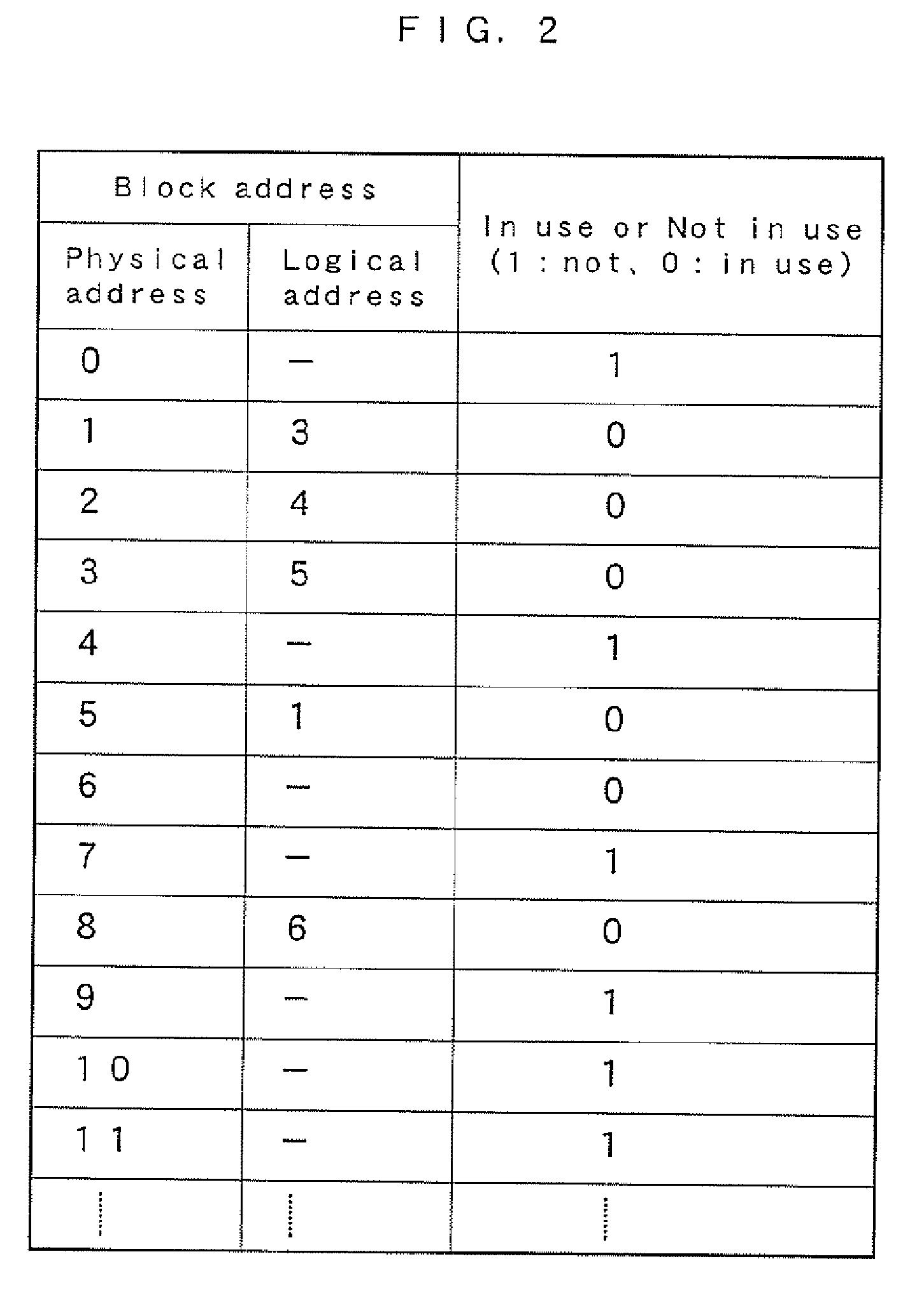
[0041] A memory card that is a nonvolatile storage apparatus in an embodiment of the present invention and its memory control circuit will be described below with referring figures. FIG. 1 is a block diagram showing a configuration of a memory card 1 including the memory control circuit according to the embodiment of the present invention. In FIG. 1, the memory card 1 is used by attaching to an electronic device (not shown) such as a digital still camera (DSC) and personal computer (PC). The memory card 1 mainly includes a host interface 2, controller 3, RAM 4, instruction ROM 5, buffer memory 6, and rewritable nonvolatile memory, for example, a flash memory 7. A part including the controller 3, RAM 4, instruction ROM 5, and buffer memory 6 is referred to as a memory control circuit.

[0042] The host interface 2 executes an interface with an electronic device body (hereinafter referred to as a host) attaching the memory card 1, and sends and receives read / write data and commands and ...


PUM


Abstract

An address at which a writing error occurs is held, and after a completion of a series of writings, the data of the held address is read. Then, a faulty-block processing is performed only for the addresses, for which it is determined that retry of writing is required, thereby preventing an increase of faulty-blocks. This can suppress the problem that when a writing is performed in a particular flash memory, a writing error frequently occurs and a large number of faulty blocks occur.

Description

TECHNICAL FIELD [0001] The present invention relates to a memory control circuit, nonvolatile storage apparatus, and memory control method which are characterized by error processing in writing data to a rewritable nonvolatile memory. BACKGROUND ART [0002] In recent years, a memory card and equipment which carry a rewritable nonvolatile memory have been spreading. Since the memory card especially has better resistance to vibration, the memory card is expected to be increasingly used. [0003] A flash memory is a typical rewritable nonvolatile memory. Generally, data is written in units of pages and data is erased in units of erase blocks. The erase block ordinary consists of a plurality of the pages. In a following description, the page and erase block are referred to as a block. It is managed in units of blocks whether the flash memory is in use or not in use, for example, “1” is written as management data with respect to a block not in use and when data is written to the block not i...

Claims


Application Information

Patent Timeline
IPC IPC(8): G11C16/06G06F12/16
CPCG11C16/10G06F11/1068
Inventor KASAHARA, TETSUSHIIZUMI, TOMOAKINAKANISHI, MASAHIROTAMURA, KAZUAKIMATSUNO, KIMINORIINAGAKI, YOSHIHISAINOUE, MANABU
Owner PANASONIC CORP
Learn More