Methods for oriented growth of nanowires on patterned substrates

a technology of nanowires and substrates, applied in the field of nanowires, can solve the problems of inconvenient mass production, current approaches to grow and harvest nanowires, and inability to yield consistent nanowire performance characteristics

Active Publication Date: 2008-02-14
ONED MATERIAL INC
View PDF99 Cites 13 Cited by
  • Summary
  • Abstract
  • Description
  • Claims
  • Application Information

AI Technical Summary

Benefits of technology

The present invention provides methods for producing nanowires by depositing nucleating particles on a substrate material and heating them to a first temperature to form a liquid alloy droplet, which is then contacted with a first precursor gas mixture to initiate nanowire growth. The substrate material can be crystallographic silicon or amorphous materials such as silicon dioxide or silicon nitride. The first temperature is higher than the second temperature at which the alloy droplet is heated. The methods can be used to produce nanowires with a desired orientation and length. The invention also provides methods for growing nanowires at lower temperatures using plasma enhanced sputter deposition.

Problems solved by technology

A major impediment to the emergence of this new generation of electronic devices based on nanostructures is the ability to effectively grow and harvest nanowires and other nanostructures that have consistent characteristics.
Current approaches to grow and harvest nanowires do not facilitate mass production and do not yield consistent nanowire performance characteristics.

Method used


Image

  • Methods for oriented growth of nanowires on patterned substrates
  • Methods for oriented growth of nanowires on patterned substrates
  • Methods for oriented growth of nanowires on patterned substrates

Examples


Embodiment Construction

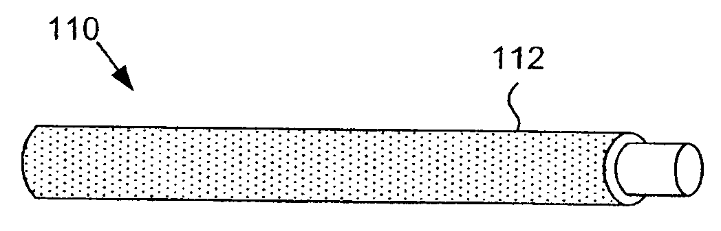
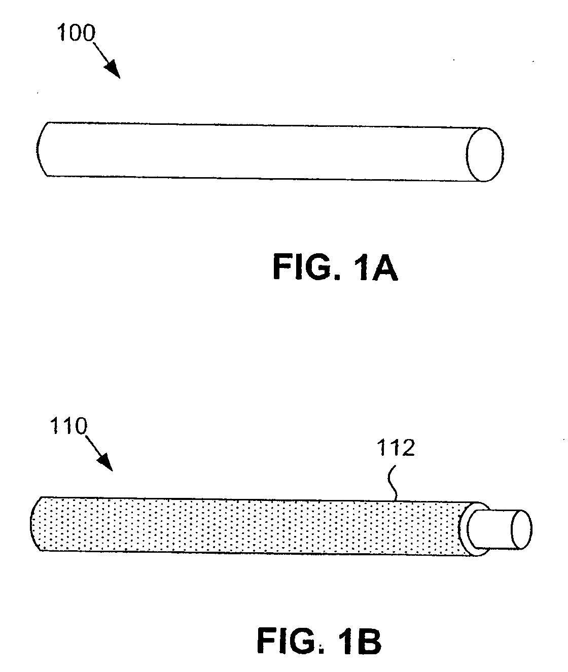
[0055] It should be appreciated that the particular implementations shown and described herein are examples of the invention and are not intended to otherwise limit the scope of the present invention in any way. Indeed, for the sake of brevity, conventional electronics, manufacturing, semiconductor devices, and nanowire (NW), nanorod, nanotube, and nanoribbon technologies and other functional aspects of the systems (and components of the individual operating components of the systems) may not be described in detail herein. Furthermore, for purposes of brevity, the invention is frequently described herein as pertaining to nanowires.

[0056] It should be appreciated that although nanowires are frequently referred to, the techniques described herein are also applicable to other nanostructures, such as nanorods, nanotubes, nanotetrapods, nanoribbons and / or combinations thereof. It should further be appreciated that the manufacturing techniques described herein could be used to create any...


PUM

PropertyMeasurementUnit
temperatureaaaaaaaaaa
temperaturesaaaaaaaaaa
length:widthaaaaaaaaaa

Abstract

The present invention is directed to systems and methods for nanowire growth and harvesting. In an embodiment, methods for nanowire growth and doping are provided, including methods for epitaxial oriented nanowire growth using a combination of silicon precursors, as well as us of patterned substrates to grow oriented nanowires. In a further aspect of the invention, methods to improve nanowire quality through the use of sacrifical growth layers are provided. In another aspect of the invention, methods for transferring nanowires from one substrate to another substrate are provided.

Description

CROSS REFERENCE TO RELATED APPLICATIONS [0001] This application claims the benefit of U.S. Provisional Patent Application No. 60 / 754,519, filed Dec. 29, 2005, the disclosure of which is incorporated herein by reference in its entirety.BACKGROUND OF THE INVENTION [0002] 1. Field of the Invention [0003] The present invention relates to nanowires, and more particularly, to nanowire growth and harvesting. [0004] 2. Background of the Invention [0005] Nanostructures, and in particular, nanowires have the potential to facilitate a whole new generation of electronic devices. A major impediment to the emergence of this new generation of electronic devices based on nanostructures is the ability to effectively grow and harvest nanowires and other nanostructures that have consistent characteristics. Current approaches to grow and harvest nanowires do not facilitate mass production and do not yield consistent nanowire performance characteristics. [0006] What are needed are systems and methods to...

Claims


Application Information

Patent Timeline
Patent Type & Authority Applications(United States)
IPC IPC(8): B32B15/02B05D5/12
CPCB82Y30/00C30B11/12Y10T428/24917C30B29/605C30B29/06B82B1/00B82Y40/00H01L21/20
Inventor PAN, YAOLINGDUAN, XIANGFENGDUBROW, ROBERT S.GOLDMAN, JAYMOSTARSHED, SHAHRIARNIU, CHUNMINGROMANO, LINDA T.STUMBO, DAVID P.FISCHER-COLBRIE, ALICESAHI, VIJENDRAROBBINS, VIRGINIA
Owner ONED MATERIAL INC
Why Eureka
Try Eureka