Flash memory system and data writing method thereof

a flash memory and data writing technology, applied in the field of flash memory systems, can solve the problems of increasing overall processing time or complicated hardware for generating parity codes, and achieve the effect of increasing the efficiency of writing and accelerating the overall processing tim

Active Publication Date: 2008-01-31
SAMSUNG ELECTRONICS CO LTD
View PDF1 Cites 30 Cited by
  • Summary
  • Abstract
  • Description
  • Claims
  • Application Information

AI Technical Summary

Benefits of technology

[0014] The present invention provides a flash memory system, which increases the efficiency of writing and reading data and parity codes into and from a flash memory device to expedite overall data processing time, and a data writing method thereof.

Problems solved by technology

Thus, with increasing the size of the page buffer, hardware for generating parity codes becomes more complicated or overall processing time increases.

Method used


Image

  • Flash memory system and data writing method thereof
  • Flash memory system and data writing method thereof
  • Flash memory system and data writing method thereof

Examples


Embodiment Construction

[0025] The present invention will now be described more fully with reference to the accompanying drawings, in which exemplary embodiments of the invention are shown. Like reference numerals are used to denote like elements throughout the drawings.

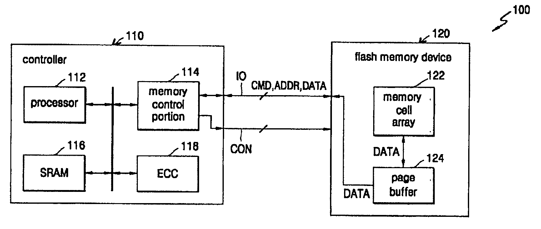
[0026] Referring to FIG. 1, a flash memory system 100 comprises a controller 110 and a flash memory device 120.

[0027] The controller 110 comprises a processor 112, a memory control portion 114, and an Error Correcting / Correction Code (“ECC”) circuit 118. The processor 112 controls the operation of the controller 110, and the memory control portion 114 interfaces the controller 110 with the flash memory device 120.

[0028] The ECC circuit 118 generates parity codes to check and / or correct the errors of data to be written in the flash memory device 120. The ECC circuit 118 is realized by hardware. As shown in FIG. 1, the controller 110 may further comprise an SRAM 116 for writing data.

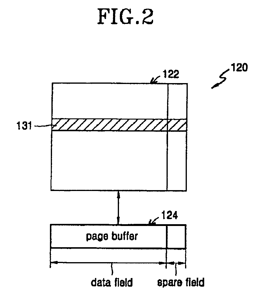
[0029] The flash memory device 120 comprises a memory ce...


PUM


Abstract

Provided are a flash memory system and a data writing method thereof, the method including (a) transmitting a predetermined command and an address signal to a flash memory device included in the flash memory system, (b) transmitting data to the flash memory device, and (c) generating a parity code for the data and transmitting the parity code to the flash memory device, where the steps (b) and (c) are repeated twice or more; and where the data and the corresponding parity codes are written in a page buffer of the flash memory device irrespective of a data field and a spare field.

Description

CROSS-REFERENCE TO RELATED APPLICATION [0001] This application is a continuation application of co-pending U.S. patent application Ser. No. 10 / 869,022 (Atty. Dkt. No. 8021-235 (SS-19626-US)), filed on Jun. 16, 2004, and entitled FLASH MEMORY SYSTEM AND DATA WRITING METHOD THEREOF, the disclosure of which is incorporated herein by reference in its entirety, which, in turn, claims foreign priority under 35 U.S.C. § 119 to Korean Patent Application No. 2003-50502, filed on Jul. 23, 2003, in the Korean Intellectual Property Office, the disclosure of which is incorporated herein by reference in its entirety.BACKGROUND OF THE INVENTION [0002] 1. Field of the Invention [0003] The present invention relates to a flash memory system, and more particularly, to a method of writing and reading data and parity codes in a flash memory system. [0004] 2. Description of the Related Art [0005] In general, a flash memory device is a kind of nonvolatile electrically erasable and programmable read only m...

Claims


Application Information

Patent Timeline
Patent Type & Authority Applications(United States)
IPC IPC(8): G06F12/00G06F11/10G11C7/10G11C16/10
CPCG06F11/1032G11C7/1078G11C2207/2245G11C16/10G11C7/1087
Inventor KWON, JEONG-MI
Owner SAMSUNG ELECTRONICS CO LTD
Why Eureka
Try Eureka