Signal distribution architecture and semiconductor device
a technology of signal distribution and semiconductor devices, applied in semiconductor devices, generating/distributing signals, oscillators, etc., can solve the problems of insufficient amplitude for a viable clock signal, difficult reception of clock signals by receiving circuits, and large differences in the standing wave amplitude of the distribution network, so as to achieve low jitter, low skew, and reduced transmission line length
Inactive Publication Date: 2007-12-13
LONGITUDE SEMICON S A R L
View PDF3 Cites 23 Cited by
- Summary
- Abstract
- Description
- Claims
- Application Information
AI Technical Summary
Benefits of technology
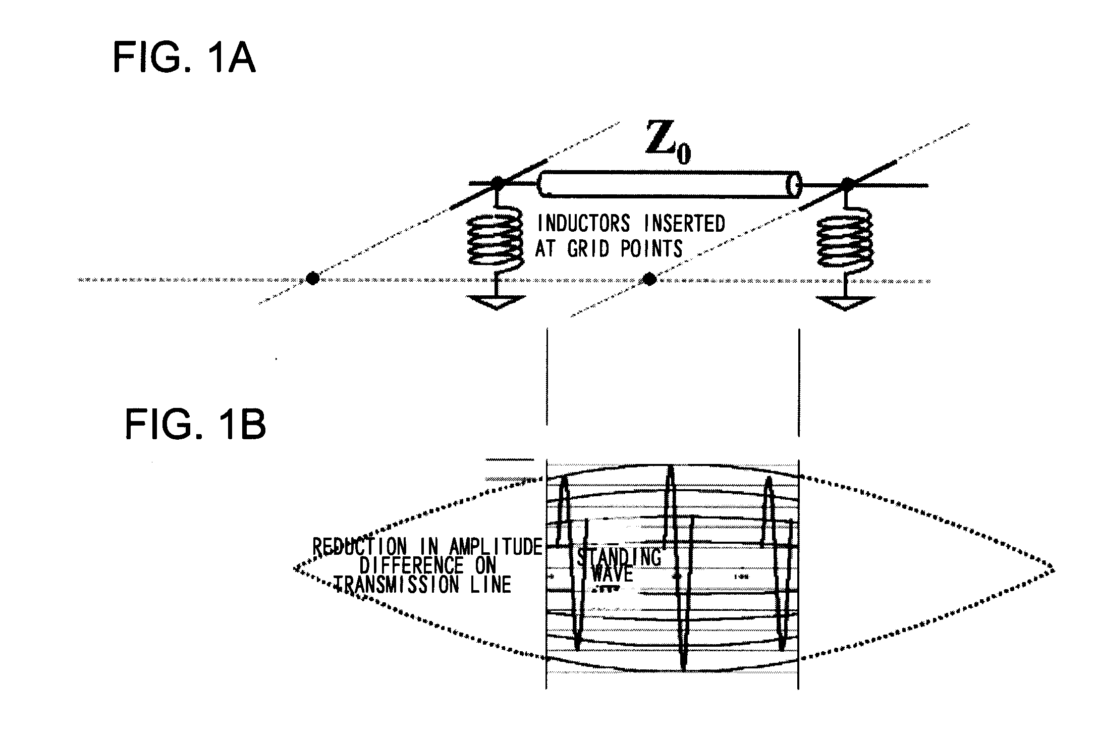
[0025]According to the present invention, inductive loads are provided at both ends of a transmission line and a low-amplitude segment of a standing wave is eliminated, thereby freely generating a standing wave having a constant phase and a substantially uniform amplitude over the transmission line.
[0035]In the present invention, it is possible to supply a signal from any position of a complementary signal transmission line to signal-supply destination circuit.
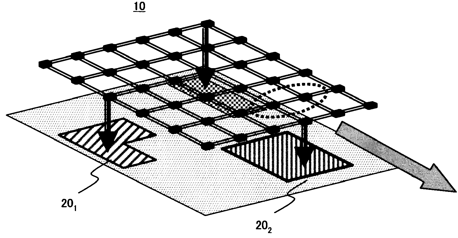
[0037]A circuit according to another aspect of the present invention uses mutual inductance as an inductance for phase compensation, and it will suffice if placement of a standing-wave path is such that the end portion thereof contacts another standing-wave path. This enables grid pitch to be set at will and enables a large reduction in the area occupied by the standing-wave supply system corresponding to the number of grid points required by the circuitry.
[0039]In accordance with the present invention, a difference in amplitude of a standing wave on a transmission line is reduced in a grid network, it is possible to supply a signal from any location, and it is possible to support scaling.
[0040]In accordance with the present invention, the length of transmission lines can be reduced to, e.g., more than one-tenth that employed with the conventional standing-wave techniques, thereby enabling a clock frequency on the order of multiple gigahertz. The invention is well suited for finer patterning. Furthermore, according to the present invention, low jitter, low skew and low power dissipation are achieved. That is, in accordance with the present invention, it is possible to transmit an ultra-high-speed clock signal in a form ideal in terms of chip area and power dissipation.
[0042]In accordance with another aspect of the present invention, mutual inductance is used as an inductance for phase compensation, and it will suffice if placement of a standing-wave path is such that the end portion thereof contacts another standing-wave path. This enables grid pitch to be set at will and enables a large reduction in the area occupied by the standing-wave supply system corresponding to the number of grid points required by the circuitry. The present invention contributes a reduction in occupied area and power dissipation.
Problems solved by technology
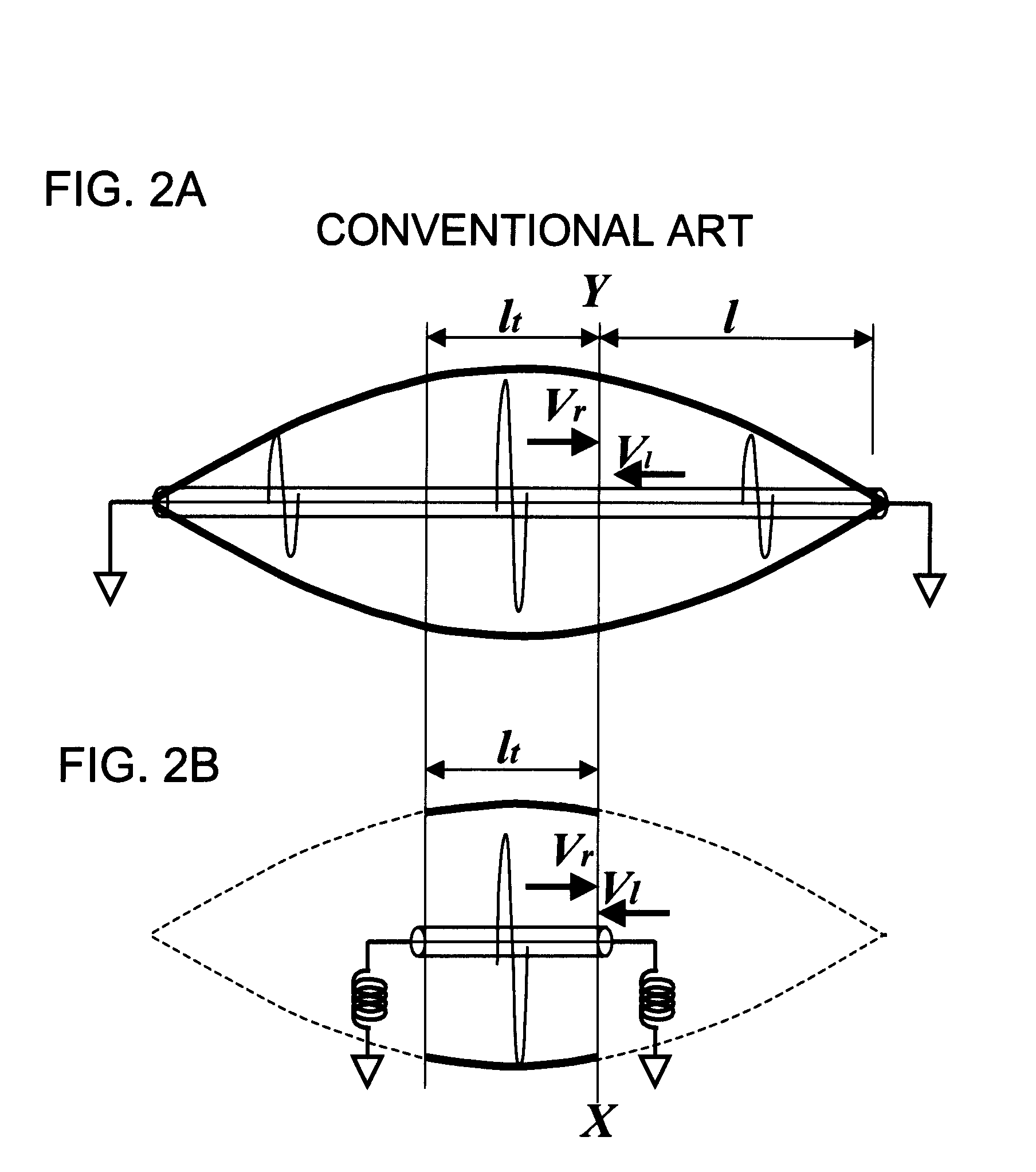
A problem with the conventional grid-type clock distribution networks using standing waves in Non-Patent Document 4, etc., is that standing-wave amplitude in the distribution network differs greatly depending upon the spatial position on a transmission line. FIG. 9A illustrates a conventional transmission line and FIG. 9B a standing wave in the transmission line.
As illustrated in FIG. 9B, depending upon position along the transmission line, amplitude for a viable clock signal is inadequate.
Consequently, reception of a clock signal by a receiving circuit is difficult in this region of inadequate amplitude and, hence, the clock is not supplied to the synchronized elements.
That is, because the standing waves on each of the transmission lines of the grid network undergo a major change in amplitude depending upon spatial position along the transmission lines, a limitation is imposed upon the locations at which driven circuits are placed.
In a mesh structure using a standing-wave clock oscillator, it is difficult to reduce grid pitch.
That is, since frequency control is uniquely decided by transmission-line length, a limitation is imposed with regard to scaling.
Method used
View moreImage
Smart ImageViewing Examples

Examples
example 1
[0086]6×6 grid size;[0087]Area: 2.4 mm×2.4 mm;[0088]Frequency: 20 GHz;[0089]Process: 0.18 μm;[0090]Power consumption: (6×6)×6 (mA)×1.8 V=0.389 W@20 GHz [19.4 mW / GHz]
[0091]Example 1 will be described in contrast to with comparison examples.
[0092]The specifications of the standing-wave scheme according to Non-Patent Document 4 are illustrated as Comparison Example 1.
Login to View More PUM
 Abstract
Provided is a grid-type high-speed clock signal distribution network capable of reducing a difference in amplitude of a standing wave on a transmission line and of supplying a signal from any position. The network for transmitting the clock signal is such that ends of the differential signal transmission line are connected via an inductor, a low-amplitude segment is eliminated by a phase shift in the inductor and a standing wave of substantially uniform phase and amplitude is produced, wherein the number of lines connected to the grid point is made the same for entire grid points.
Description
FIELD OF THE INVENTION[0001]This invention relates to the structure of a signal transmission line and, more particularly, to a signal distribution architecture ideal for application to transmission of high-speed signals and to a semiconductor device having this signal distribution architecture.BACKGROUND OF THE INVENTION[0002]Clock frequencies used in large-scale integrated circuits (LSI circuits) have reached the gigahertz band in recent years. In an LSI circuit, clock signal is distributed to all clock synchronous elements via a clock distribution network (wirings and buffer circuits, etc.). Tree-type and grid-type clock distribution arrangements have long been used as typical means for clock distribution adapted to reduce a phase difference at the clock terminals of the clock-synchronous elements within an LSI circuit.[0003]With the tree (H-tree) arrangement, the clock branches in the form of a tree and is supplied to the clock synchronous elements (load circuits) from a centrall...
Claims
Login to View More Application Information
Patent Timeline
 IPC IPC(8): H03B9/14
CPCH03B5/1841G06F1/10H01L2924/0002H01L2924/00
Inventor IKEDA, HIROAKISASAKI, MAMORUIWATA, ATSUSHISHIOZAKI, MITSURUMORI, ATSUSHI
Owner LONGITUDE SEMICON S A R L
Features
- R&D
- Intellectual Property
- Life Sciences
- Materials
- Tech Scout
- Unparalleled Data Quality
- Higher Quality Content
- 60% Fewer Hallucinations
Learn More Browse by: Latest US Patents, China's latest patents, Technical Efficacy Thesaurus, Application Domain, Technology Topic, Popular Technical Reports.
© 2025 PatSnap. All rights reserved.Legal|Privacy policy|Modern Slavery Act Transparency Statement|Sitemap|About US| Contact US: help@patsnap.com