Method for packaging integrated circuit dies

Inactive Publication Date: 2007-12-06
HOCK LIN TIANG
View PDF13 Cites 4 Cited by
  • Summary
  • Abstract
  • Description
  • Claims
  • Application Information

AI Technical Summary

Benefits of technology

[0012] The invention may provide a number of advantages. Firstly, the number of packages that can be produced in a single molding operation is doubled, dramatically producing productivity.
[0014] This leads to a third advantage, which is that since the substrates support each other, such that the combination of the two substrates is more rigid than a single substrate, each of the substrates can be thinner than in conventional systems without risk of them being damaged.
[0016] Further, the channel(s) that introduce(s) resin into the cavity or cavities open into the cavity at a location spaced from the surface of the substrate. Thus, the gates are not formed directly on the substrate, and do not become adhered to it. This makes the degating operation much simpler.
[0019] Furthermore, since the gates are not formed on the substrate none of the substrate area is wasted as gate lands. Thus, dies can be located close to the edge of the substrate (or at least closer than in the conventional system). From one point of view, this means that for a given number of dies the area of the required substrate is less, leading to reduced costs (particularly since typically the substrate is selectively gold plated). From another point of view, for a given size of the substrate, this means that the proportion of the substrate that can be utilized is increased.

Problems solved by technology

There are several disadvantages with this molding technique.
This may result in the electrical connections from the lower surface of the substrate 3 being lost.
Secondly, substrates are now becoming thinner, which makes handling them during the molding operation progressively more difficult.
Another disadvantage of the known technique is that the gate 11 has to be removed from the package before the package is used (“degating”).

Method used


Image

  • Method for packaging integrated circuit dies
  • Method for packaging integrated circuit dies
  • Method for packaging integrated circuit dies

Examples


Embodiment Construction

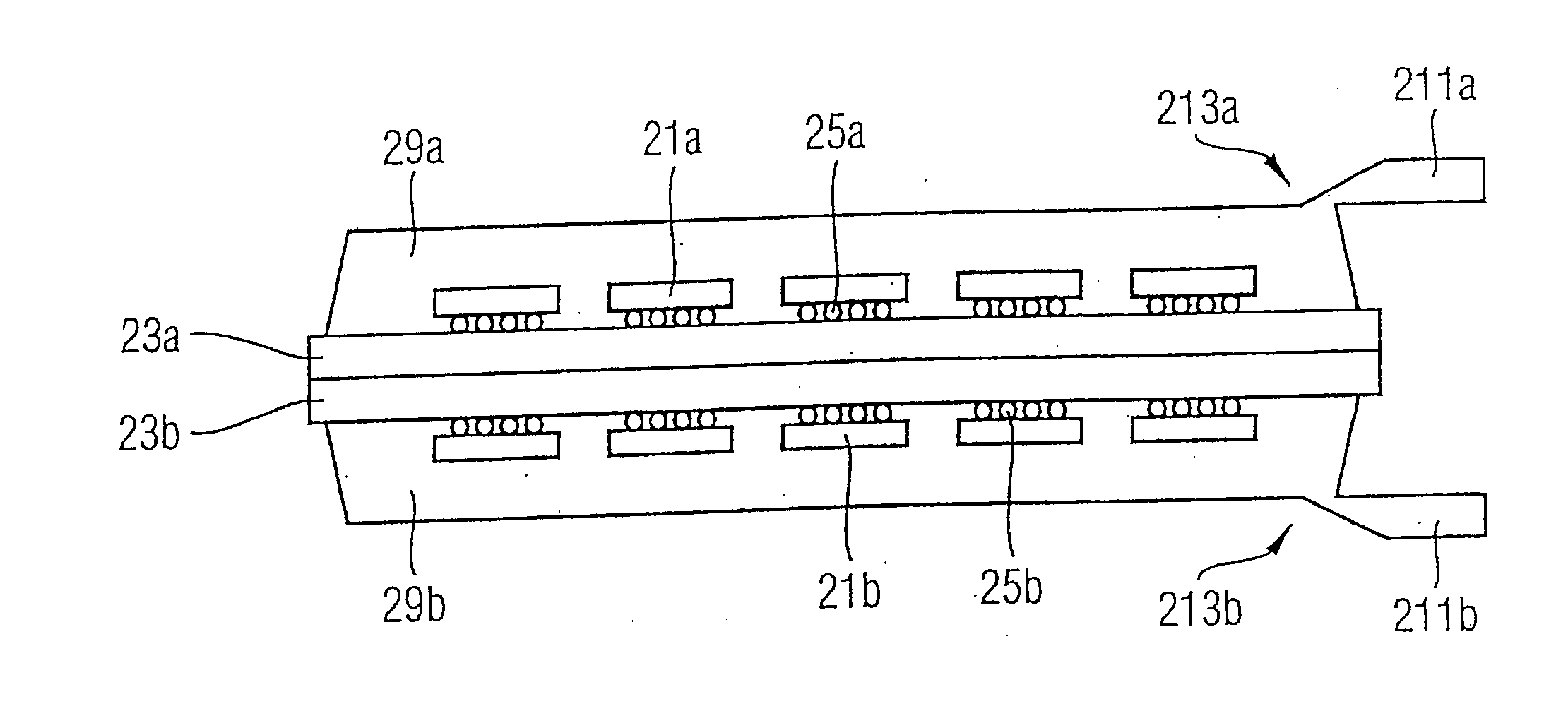
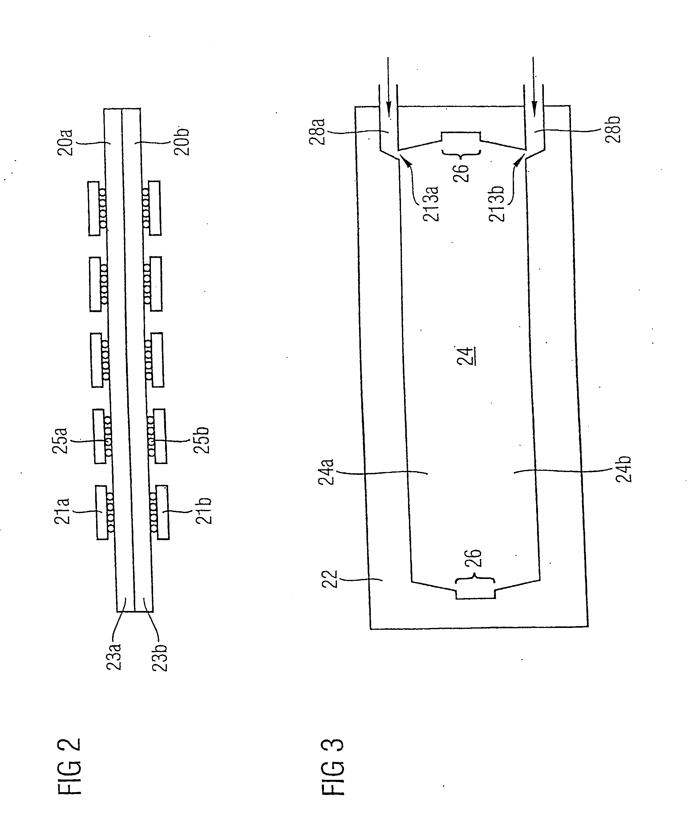
[0028] Referring to FIG. 2, the first step of a method which is an embodiment of the invention is shown. In the molding method, the two substrates 23a, 23b are each of the kind shown in FIG. 1. These substrates may, for example, be printed circuit boards, or otherwise include electrical circuitry, extending, for example, parallel to the major surfaces of the substrate. Their surfaces 20a, 20b carry dies 21a, 21b connected to the substrates 23a, 23b by a ball grid array (BGA), e.g., of eutectic solder balls 25a, 25b. The substrates 23a, 23b are placed in a back-to-back configuration, so that their back faces are in contact, and their front faces 20a, 20b, carrying dies 21a, 21b, are directed in opposite directions.

[0029] As shown in FIG. 3, the substrates 23a, 23b are placed in this configuration into a mold cavity 24 in a mold chase 22, such that the cavity 24 is divided into two cavities 24a, 24b (in FIG. 3, these are respectively the upper and lower portions 24a, 24b of the cavit...


PUM


Abstract

A packaging method is proposed in which two substrates 23a, 23b, each carrying at least one die 21a, 21b, are placed back-to-back in a mold chase 22 with their surfaces 20a, 20b, which carry dies, facing into respective cavities 24a, 24b. Each cavity is fed liquid resin through at least one respective channel 28a, 28b that introduces the resin into the cavity at a location spaced from the corresponding substrate. Thus a resin body 29a, 29b is formed on each of the substrates 23a, 23b. Thus, a package is produced from each of the two substrates 23a, 23b in a single molding operation. The invention is particularly suitable for producing flip-chip-in-package type packages.

Description

[0001] This application is a continuation of co-pending International Application No. PCT / SG2004 / 000426, filed Dec. 24, 2004, which designated the United States and was published in English, and which is based on Singapore Application No. 200400083-2 filed Jan. 6, 2004, both of which applications are incorporated herein by reference.TECHNICAL FIELD [0002] The present invention relates to methods for creating packages to packages produced by the methods. BACKGROUND [0003] Recently there has been increasing interest in “flip-chip in package” (FCIP) components, that is integrated circuits in which the die is interconnected to the lead structure of the package as a flip-chip. The die is formed with electrical contacts on a surface that is turned towards a substrate, and connected to it such that the electrical contacts on the die are electrically connected to respective contracts of the substrate. Normally this is done by providing a ball grid array (BGA) on the surface of the die. Afte...

Claims


Application Information

Patent Timeline
IPC IPC(8): B05C3/12H01L21/56H01L23/31
CPCH01L21/565H01L23/3128H01L25/0652H01L2224/16225H01L2924/01322H01L2224/16227H01L2924/00
Inventor HOCK, LIN TIANG
Owner HOCK LIN TIANG
Why Eureka
Try Eureka