Array Substrate and Liquid Crystal Display Panel
a liquid crystal display and substrate technology, applied in non-linear optics, instruments, optics, etc., can solve the problems of limited viewing angle, serious viewing angle problem, and inability to provide uniform gray scale in lcd, so as to reduce color shift and contrast the effect of decreasing, uniform gray scale and simple structural adjustmen
- Summary
- Abstract
- Description
- Claims
- Application Information
AI Technical Summary
Benefits of technology
Problems solved by technology
Method used
Image

Examples
embodiment 1
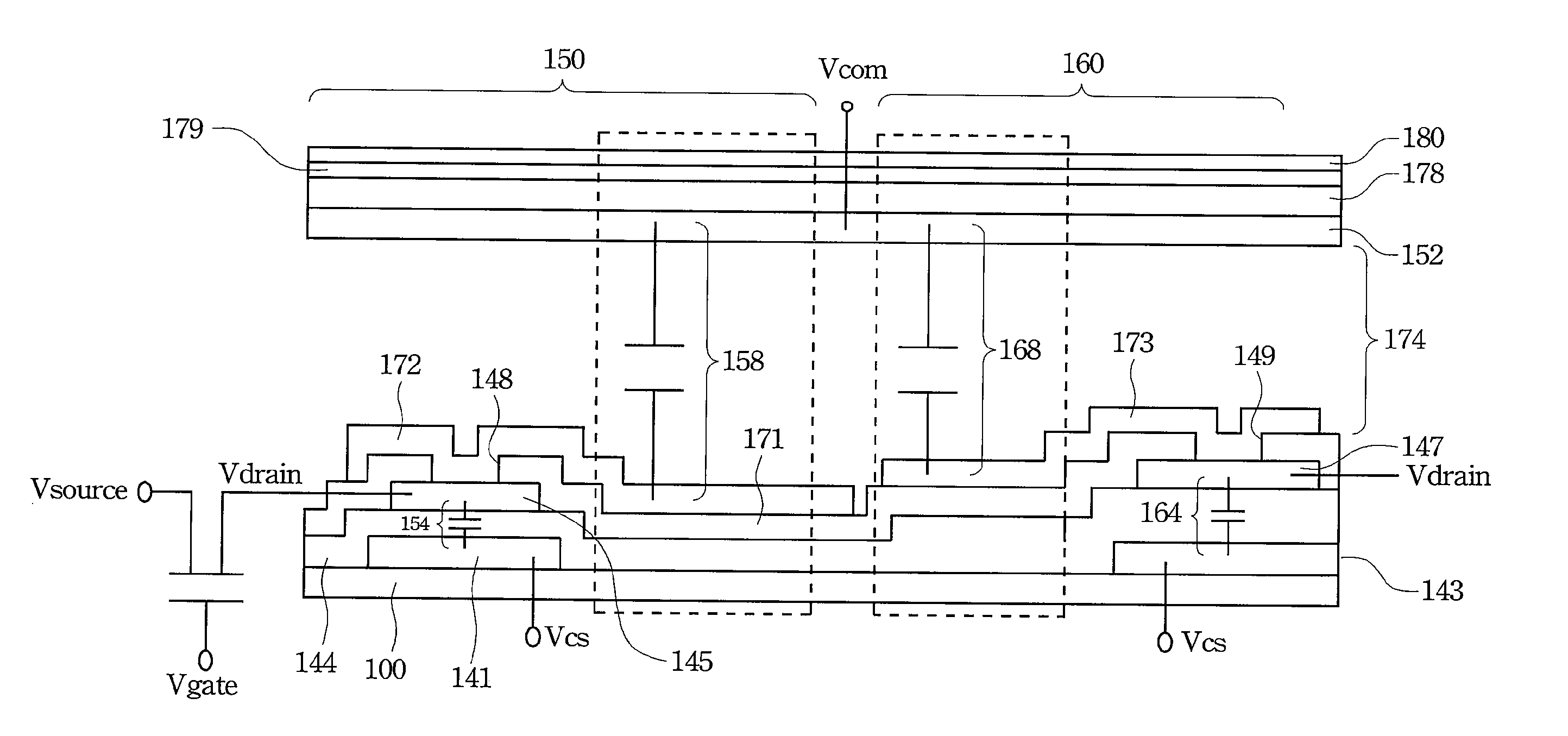
[0019]FIG. 1 is a cross-sectional view of a pixel of a LCD panel according to the embodiment 1 of the invention. In FIG. 1, the pixel region is further divided into two sub-pixel regions. The left side of the cross-sectional view of FIG. 1 is a first sub-pixel region 150, and the right side of the cross-section view is a second sub-pixel region 160. The area of the first sub-pixel region 150 can be unequal to the area of the second sub-pixel region 160. Base on the required viewing angle effect, the areas of the first sub-pixel region 150 and the second sub-pixel region 160 can be adjusted. A lower electrode is disposed over the first substrate 100 cross the first sub-pixel region 150 and the second sub-pixel region 160. To facilitate distinguishing, a portion of the lower electrode in the first sub-pixel region 150 is called the first lower electrode 141, and the other portion of the lower electrode in the second sub-pixel region 160 is called the second lower electrode 143. A diel...
embodiment 2
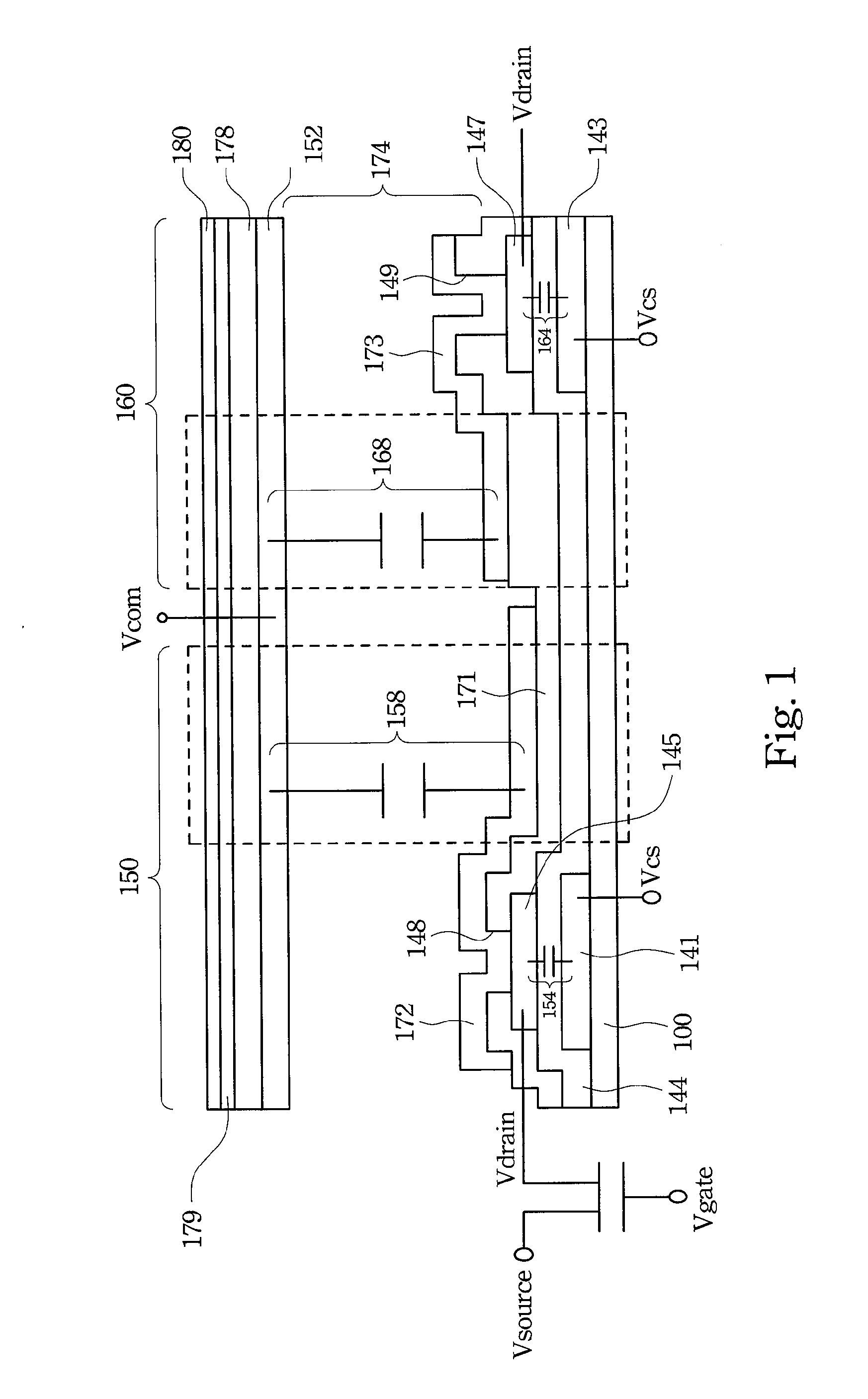
[0025]The major difference between embodiment 1 and embodiment 2 is the cross-sectional structure. FIG. 2 is a cross-sectional view of a single pixel of a LCD panel according to the embodiment 2 of the invention. In FIG. 2, the element structures identical to those described in the embodiment 1 can be directly referred to the description of the embodiment 1 and won't be repeated here. The description of the embodiment 2 focuses on the difference between the embodiment 2 and the embodiment 1. In the embodiment 1, the different capacitance values of the pixel capacitors of the different sub-pixels are achieved by adjusting the thickness of the passivation layer in the sub-pixels to modify the thickness of the liquid crystal layer in the pixel capacitors of the sub-pixels. In the embodiment 2, the thickness of the passivation layer in the sub-pixels is fixed. Instead of adjusting the thickness of the passivation layer, the embodiment 2 adjusts the thickness of the organic layer in the ...
embodiment 3
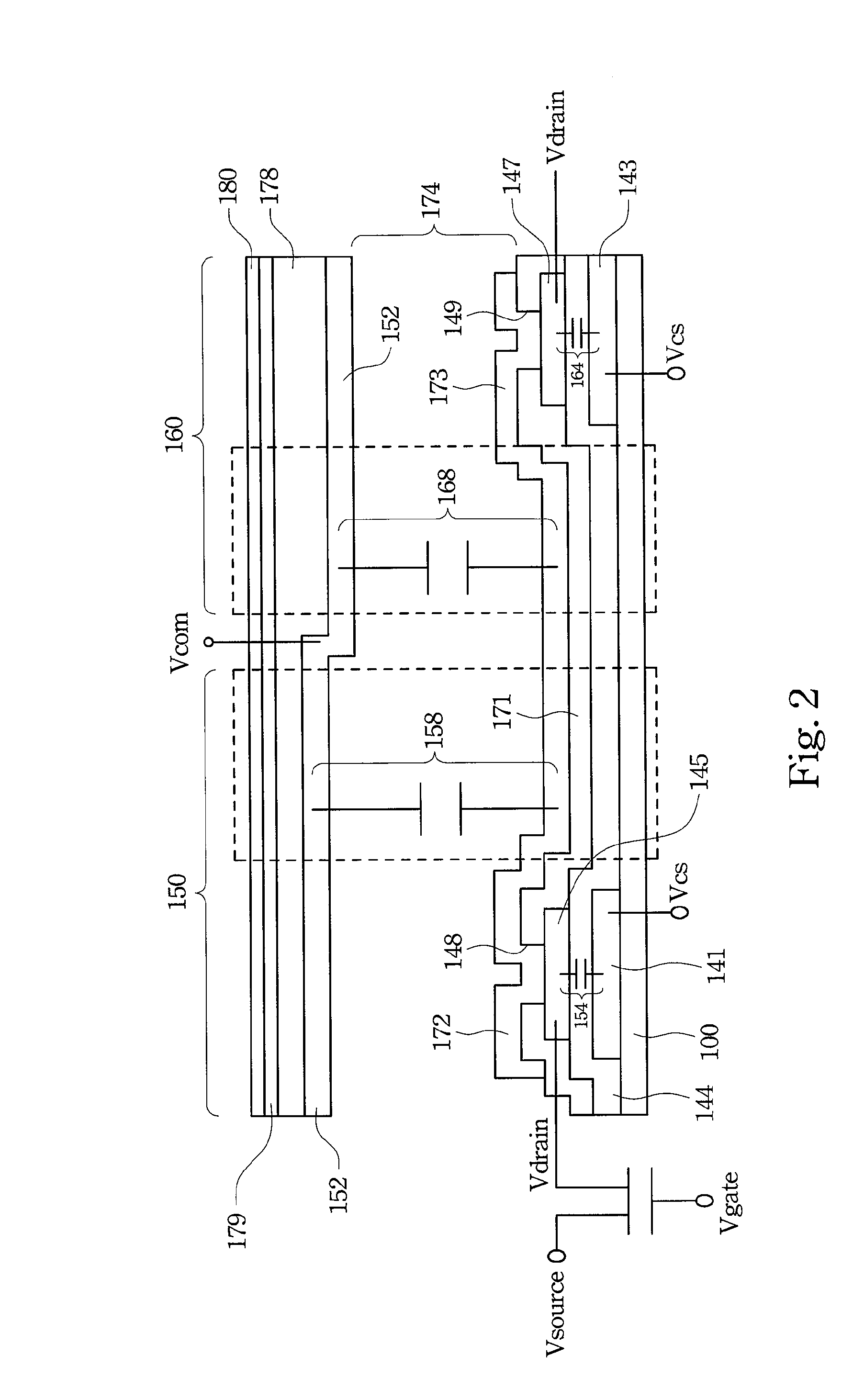
[0028]FIG. 3 is a cross-sectional view of a single pixel of a LCD panel according to the embodiment 3 of the invention. In FIG. 3, the element structures identical to those described in the embodiment 1 can be directly referred to the description of the embodiment 1 and won't be repeated here. The total capacitance value of the pixel is the sum of the capacitance values of the storage capacitor, the pixel capacitor and other coupling capacitor. In the embodiment 1 and the embodiment 2, the different total capacitance values of the different sub-pixels are achieved by changing the capacitance values of the pixel capacitors of the sub-pixels. Different from previous two embodiments, the embodiment 3 achieves different total capacitance values of different sub-pixels by changing the capacitance values of the storage capacitors of the sub-pixels.
[0029]Therefore, in this embodiment, the thickness of the passivation layer 171 in the first sub-pixel region 150 is identical to the thickness...
PUM
| Property | Measurement | Unit |
|---|---|---|
| thickness | aaaaa | aaaaa |
| area | aaaaa | aaaaa |
| viewing angle | aaaaa | aaaaa |
Abstract
Description
Claims
Application Information
 - R&D
- Intellectual Property
- Life Sciences
- Materials
- Tech Scout
- Unparalleled Data Quality
- Higher Quality Content
- 60% Fewer Hallucinations
Browse by: Latest US Patents, China's latest patents, Technical Efficacy Thesaurus, Application Domain, Technology Topic, Popular Technical Reports.
© 2025 PatSnap. All rights reserved.Legal|Privacy policy|Modern Slavery Act Transparency Statement|Sitemap|About US| Contact US: help@patsnap.com