
Flat-panel type display and spacer

Inactive Publication Date: 2007-11-22
SONY CORP
View PDF3 Cites 18 Cited by
  • Summary
  • Abstract
  • Description
  • Claims
  • Application Information

AI Technical Summary

Benefits of technology

[0020]Accordingly, it is desirable to provide a flat-panel type display capable of reducing relative changes in brightness of pixels along a spacer provided with an antistatic coating formed from germanium nitride and a spacer to be used in a flat-panel type display.
[0079]According to the spacer of an embodiment of the present invention, since the antistatic coating is formed from germanium nitride containing no transition element, variations in electrical resistance due to collision of electrons may be reduced. When the thickness of the antistatic coating is specified to be within the range of 2 nm to 20 nm and the volume resistivity of the substrate of spacer is specified to be within the range of 5×10⁶ Ω·m to 2×10⁸ Ω·m, the electrical charge due to charging may be passed to the anode panel side or the cathode panel side without a hitch. According to the flat-panel type display of an embodiment of the present invention, a flat-panel type display capable of reducing changes in brightness, which occur in pixels along a spacer, may be obtained.

Problems solved by technology

Therefore, the display may be damaged by atmospheric pressure unless the spacers 40 are disposed between the anode panel AP and the cathode panel CP.

Method used


Image

  • Flat-panel type display and spacer
  • Flat-panel type display and spacer
  • Flat-panel type display and spacer

Examples


example

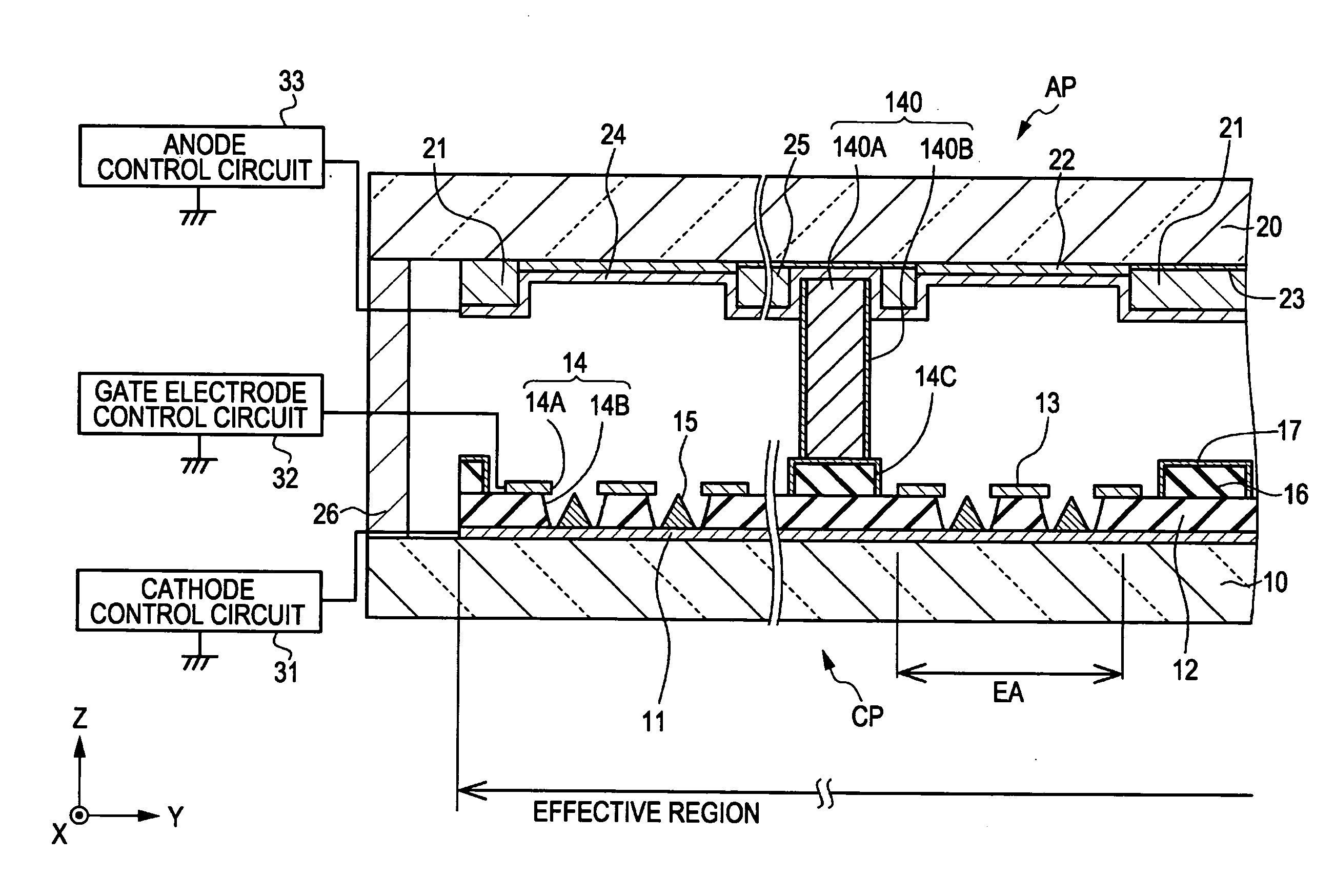
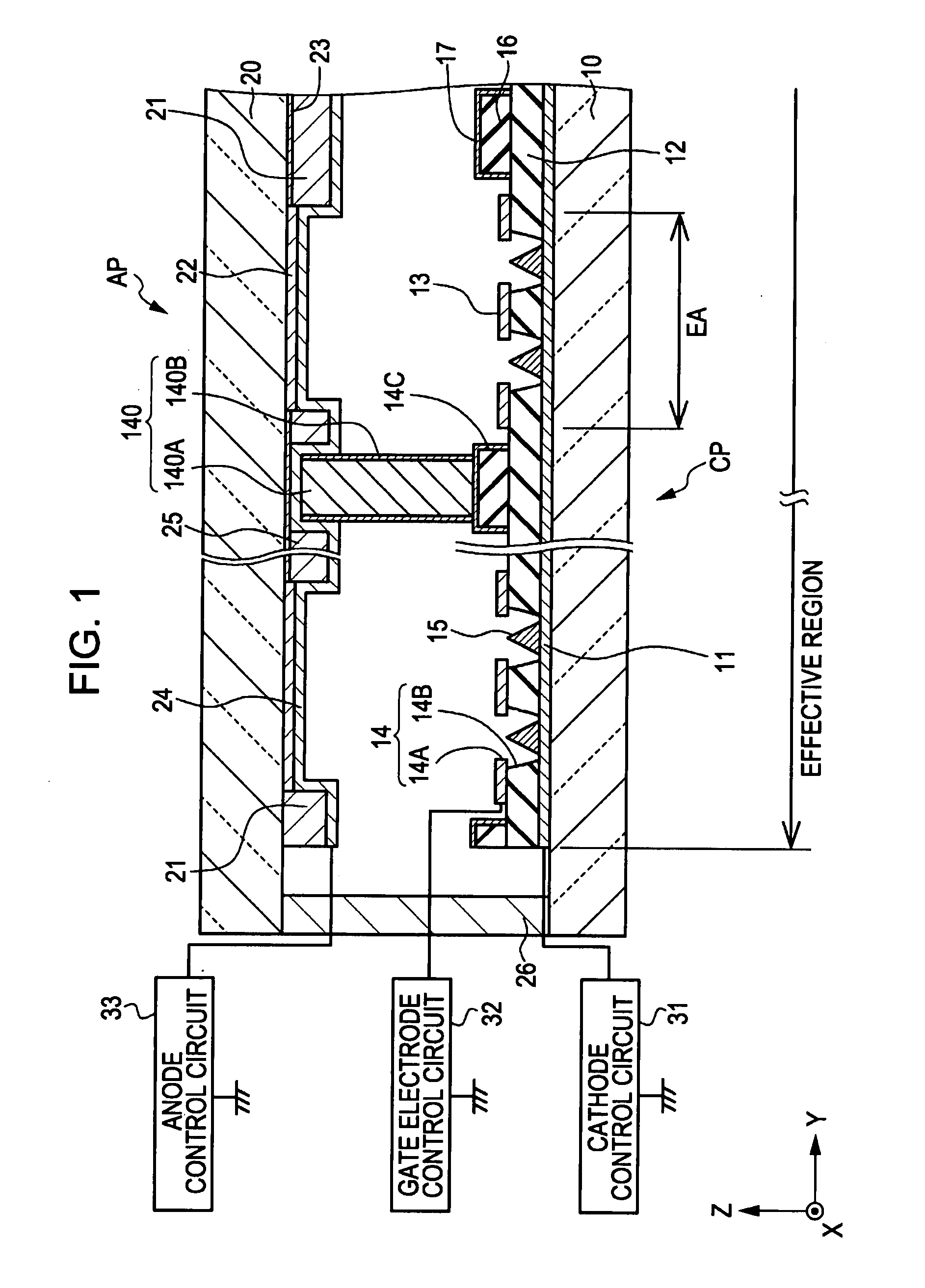
[0089]Example is related to a flat-panel type display according to an embodiment of the present invention and a spacer according to an embodiment of the present invention. FIG. 1 is a conceptual partial end view of a flat-panel type display of Example. The flat-panel type display of Example is a cold-cathode field electron emission display (hereafter abbreviated as a display) similarly to the display described in Related Art.

[0090]In the display of Example, a schematic perspective exploded view of a part of a cathode panel CP and an anode panel AP when the cathode panel CP and the anode panel AP are disassembled is similar to the diagram shown in FIG. 6.

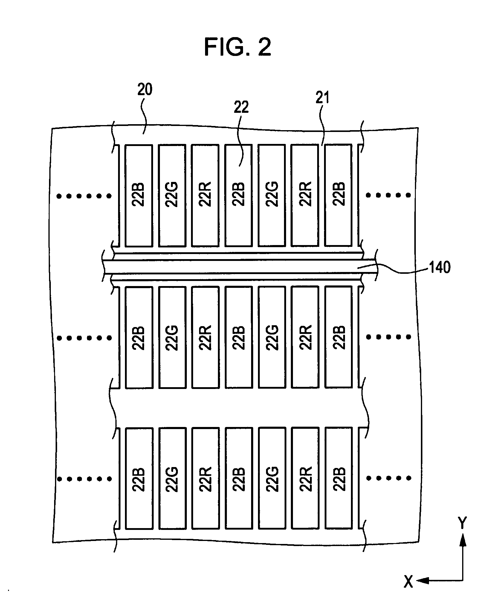
[0091]In the display of Example, a marginal portion of a cathode panel CP provided with a plurality of electron emission regions EA and a marginal portion of an anode panel AP provided with luminescent layers 22 and an anode 24 are bonded to each other, spacers 140 are disposed between the cathode panel CP and the anode panel AP, and...


PUM


Abstract

A flat-panel type display is provided, in which a marginal portion of a cathode panel provided with a plurality of electron emission regions and a marginal portion of an anode panel provided with luminescent layers and an anode are bonded to each other, spacers are disposed between the cathode panel and the anode panel, and a space sandwiched between the cathode panel and the anode panel is maintained under vacuum. The spacer includes a substrate of spacer and an antistatic coating disposed on the side surface of the spacer material, wherein the antistatic coating is formed from germanium nitride containing no transition metal, the thickness of the antistatic coating is within the range of 2 nm to 20 nm, and the volume resistivity of the substrate of spacer is within the range of 5×10⁶ Ω·m to 2×10⁸ Ω·m.

Description

CROSS REFERENCES TO RELATED APPLICATIONS[0001]The present invention contains subject matter related to Japanese Patent Application JP 2006-137398 filed in the Japanese Patent Office on May 17, 2006, the entire contents of which are incorporated herein by reference.BACKGROUND OF THE INVENTION[0002]1. Field of the Invention[0003]The present invention relates to a spacer to be used in a flat-panel type display and a flat-panel type display incorporated with the spacer.[0004]2. Description of the Related Art[0005]Various flat-panel type displays have been researched as image displays alternative to the cathode ray tube (CRT). Examples of such flat-panel type displays may include a liquid crystal display (LCD), an electroluminescent display (ELD), and a plasma display panel (PDP). Furthermore, a flat-panel type display incorporated with an electron emission element is under development. Cold-cathode field electron emission elements, metal / insulating film / metal type elements (may be refer...

Claims


Application Information

Patent Timeline
IPC IPC(8): H01J19/42H01J63/04
CPCH01J29/864H01J29/88H01J2329/865H01J2329/864H01J2329/8645H01J31/127
Inventor SEKI, ATSUSHI
Owner SONY CORP
Learn More