
Lateral double-diffused metal oxide semiconductor (LDMOS) device with an enhanced drift region that has an improved Ron area product

a metal oxide semiconductor and lateral technology, applied in the field of lateral double-diffused metal oxidesemiconductors (ldmos) transistors, can solve the problems of increasing the on-resistance of the ldmos transistor and high on-resistance, and achieve the effect of significantly reducing the on-resistance and the product of the ron*area area

Active Publication Date: 2007-10-25
MICREL
View PDF8 Cites 36 Cited by
  • Summary
  • Abstract
  • Description
  • Claims
  • Application Information

AI Technical Summary

Benefits of technology

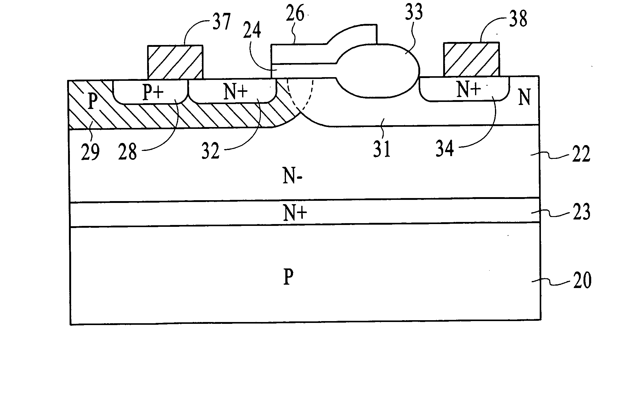
[0009] By designing the LDMOS device such that the enhanced drift region overlaps and compensates the lateral tail of the body region of the LDMOS transistor, the Ron*area product is reduced. Accordingly, the on-resistance is significantly reduced while minimally affecting the breakdown voltage of the device.

Problems solved by technology

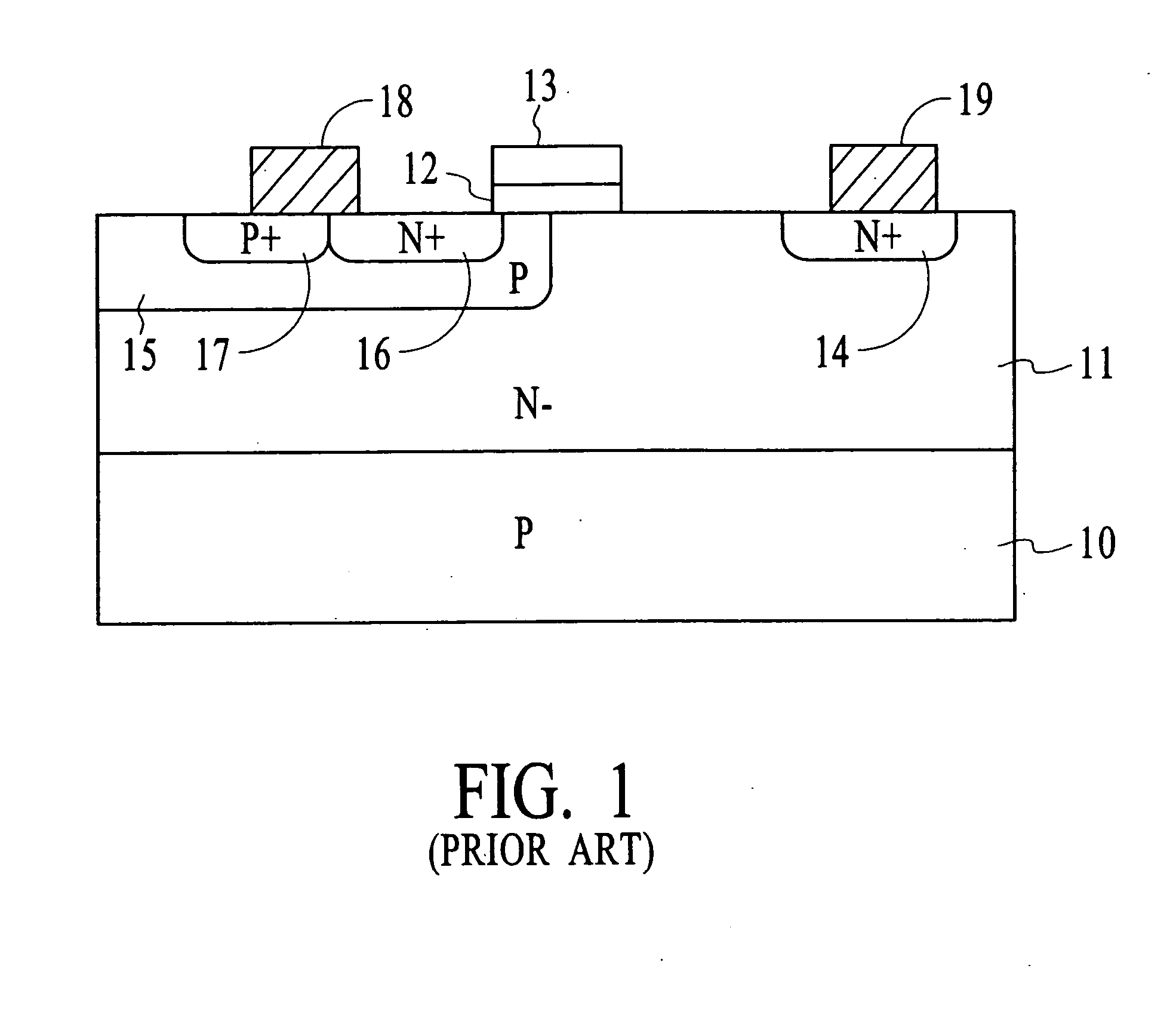
However, increasing the distance between the drain region and the gate also undesirably increases the on-resistance of the LDMOS transistor.
Therefore, in the conventional LDMOS transistor, high breakdown voltage leads to high on-resistance.

Method used


Image

  • Lateral double-diffused metal oxide semiconductor (LDMOS) device with an enhanced drift region that has an improved Ron area product
  • Lateral double-diffused metal oxide semiconductor (LDMOS) device with an enhanced drift region that has an improved Ron area product
  • Lateral double-diffused metal oxide semiconductor (LDMOS) device with an enhanced drift region that has an improved Ron area product

Examples


Embodiment Construction

[0015] The present invention relates generally to lateral double-diffused metal oxide-semiconductors (LDMOS) transistors and more particularly to an improved LDMOS transistor having a high breakdown voltage and a low on resistance. The following description is presented to enable one of ordinary skill in the art to make and use the invention and is provided in the context of a patent application and its requirements. Various modifications to the preferred embodiment and the generic principles and features described herein will be readily apparent to those skilled in the art. Thus, the present invention is not intended to be limited to the embodiment shown but is to be accorded the widest scope consistent with the principles and features described herein.

[0016] U.S. Pat. No. 5,517,046, issued to the assignee of the present application, discloses an LDMOS transistor which incorporates an enhanced drift region. In one embodiment, the transistor is formed in an N− epitaxial layer with ...


PUM


Abstract

A lateral double-diffused metal oxide semiconductor (LDMOS) device is disclosed. The LDMOS device comprises a gate region and a body region under the gate region. The LDMOS device includes an enhanced drift region under the gate region. The enhanced drift region touches the body region. By designing the device such that the enhanced drift region overlaps and compensates the lateral tail of the body region of the LDMOS transistor, the Ron*area product is reduced. Accordingly, the on-resistance is significantly reduced while minimally affecting the breakdown voltage of the device.

Description

FIELD OF THE INVENTION [0001] The present invention relates generally to lateral double-diffused metal oxide-semiconductors (LDMOS) transistors and more particularly to an improved LDMOS transistor having a high breakdown voltage and a low on resistance. BACKGROUND OF THE INVENTION [0002] Low on-resistance LDMOS transistors with high breakdown voltages are desirable for their low power loss in high voltage applications. It is well known in the art to increase breakdown voltage by increasing the distance between the drain region and the gate. However, increasing the distance between the drain region and the gate also undesirably increases the on-resistance of the LDMOS transistor. [0003]FIG. 1 is a cross-sectional view of a conventional LDMOS transistor which serves to illustrate some of the causes of the increased on-resistance. In FIG. 1, a P substrate 10 has formed over it an N− epitaxial layer 11. On the surface of N− epitaxial layer 11 is formed an oxide layer 12, on which is fo...

Claims


Application Information

Patent Timeline
Patent Type & Authority Applications(United States)
IPC IPC(8): H01L29/76H01L29/94H01L31/00
CPCH01L29/0878H01L29/0882H01L29/7816H01L29/42368H01L29/1095
Inventor MCCORMACK, STEVEYOO, JI-HYOUNG
Owner MICREL
Learn More