Optical information recording medium suppressing sulfuration of silver
a technology of optical information and recording medium, which is applied in the field of optical information recording medium suppressing sulfuration of silver, can solve the problems of increasing the cost of manufacturing optical disk, increasing the cost of optical disk manufacturing, and barrier film raising problems, so as to achieve efficient recording/reproduction operation and increase the transmission factor of layer structure
- Summary
- Abstract
- Description
- Claims
- Application Information
AI Technical Summary
Benefits of technology
Problems solved by technology
Method used
Image
Examples
example 1
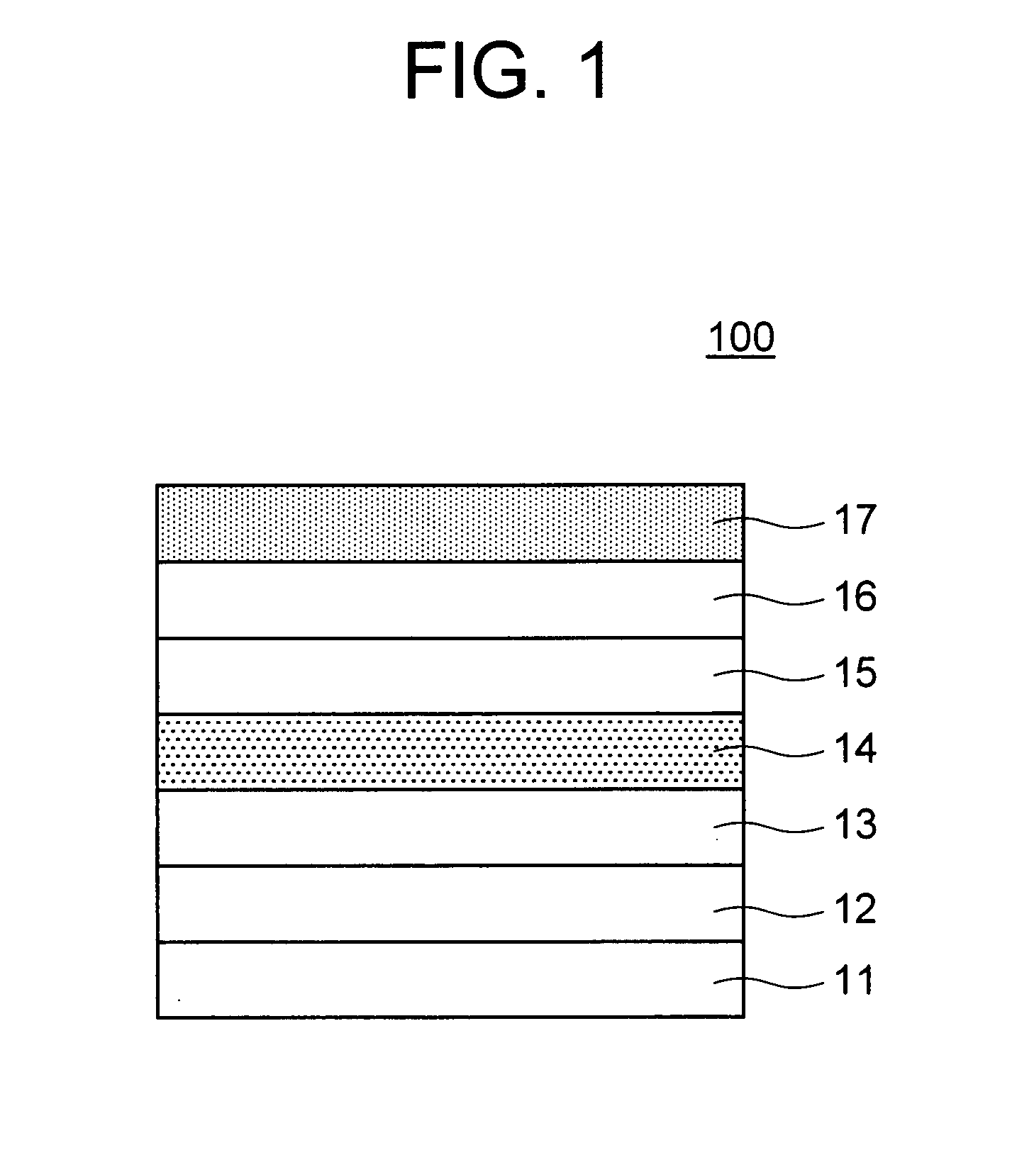
[0054] In this example, optical disks were prepared on the basis of the first embodiment as optical disks of Example 1. A polycarbonate substrate was used as the transparent substrate 11 in the optical disks of Example 1. The first dielectric film 12 was made of ZnS—SiO2 to have a film thickness of 50 nm and the recording film 14 was made of GeSbTe to have a film thickness of 12 nm whereas the first interface film 13 and the second interface film 15 were made of GeN film and the reflection film 17 was made of AgPdCu film. A variety of film compositions were used for the second dielectric film 16 to produce optical disks having a second dielectric film 16 of a variety of film compositions.
[0055] For the purpose of comparison, an optical disk having a second dielectric film 16 that is made of ZnS—SiO2 was prepared as the optical disk of Comparative Example 1. Also for the purpose of comparison, an optical disk having a reflection film 17 directly formed on the transparent substrate 1...
example 2
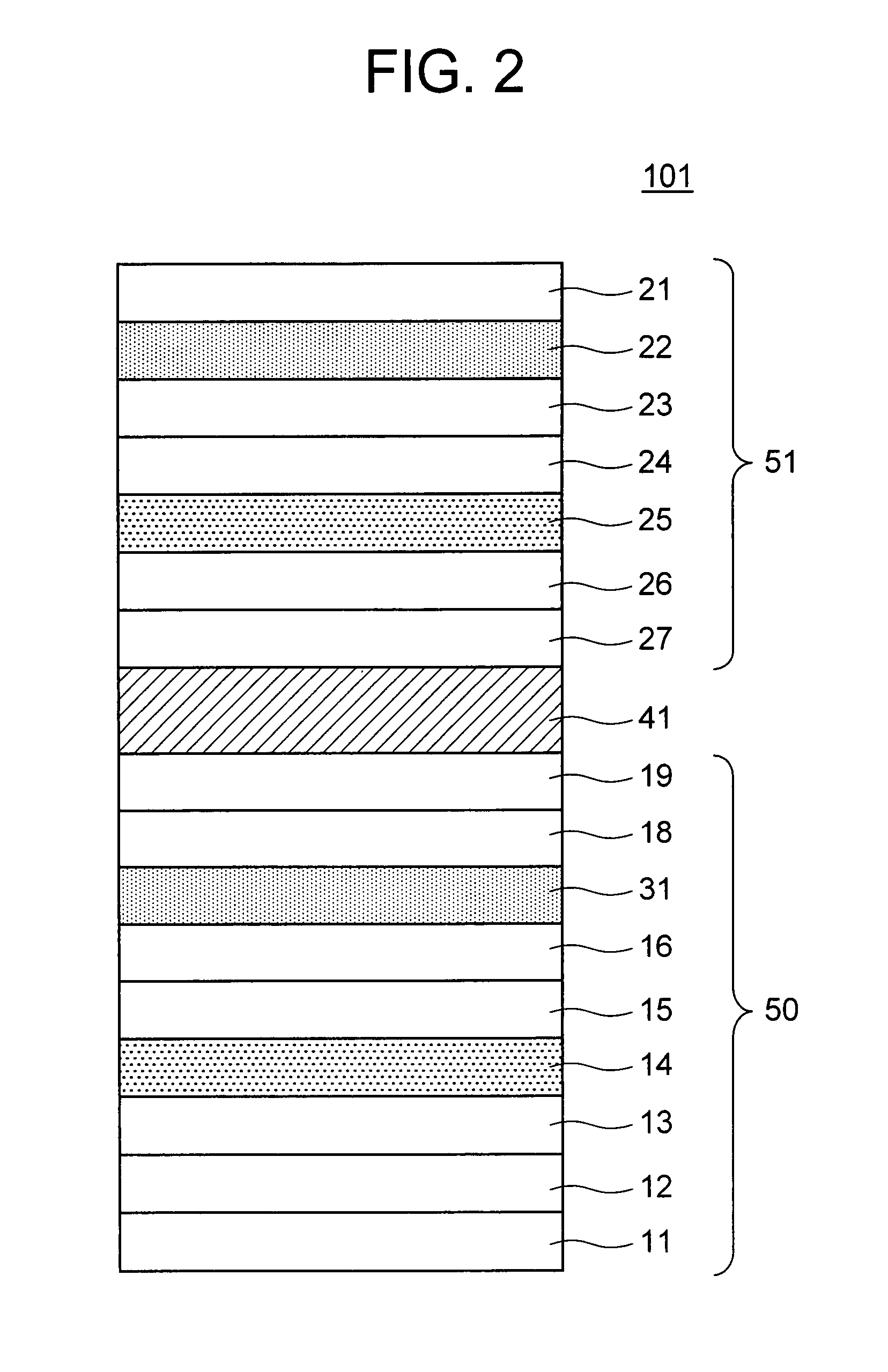
[0071] Optical disks of Example 2 were prepared by forming the first layer structure 50 according to the second embodiment and subsequently bonding the same with a dummy substrate for each optical disk. A polycarbonate substrate was used for the transparent substrate 11 of the optical disks of Example 2. The first dielectric film 12 was made of ZnS—SiO2 to have a film thickness of 50 nm and the recording film 14 was made of GeSbTe to have a film thickness of 7 nm, whereas the first interface film 13 and the second interface film 15 were made of GeN to have a film thickness of 3 nm and the semi-transmissive film 31 was made of AgPdCu to have a film thickness of 10 nm.
[0072] A film formed in Example 1 and containing Nb2O5 at 60 mol %, Al2O3 at 15 mol % and Ta2O5 at 25 mol % was selected for the second dielectric film 16, which was made to have a film thickness of 15 nm.
[0073] The fourth dielectric film 19 was made of ZnS—SiO2 to a film thickness of 110 nm. A Variety of film composit...
example 3
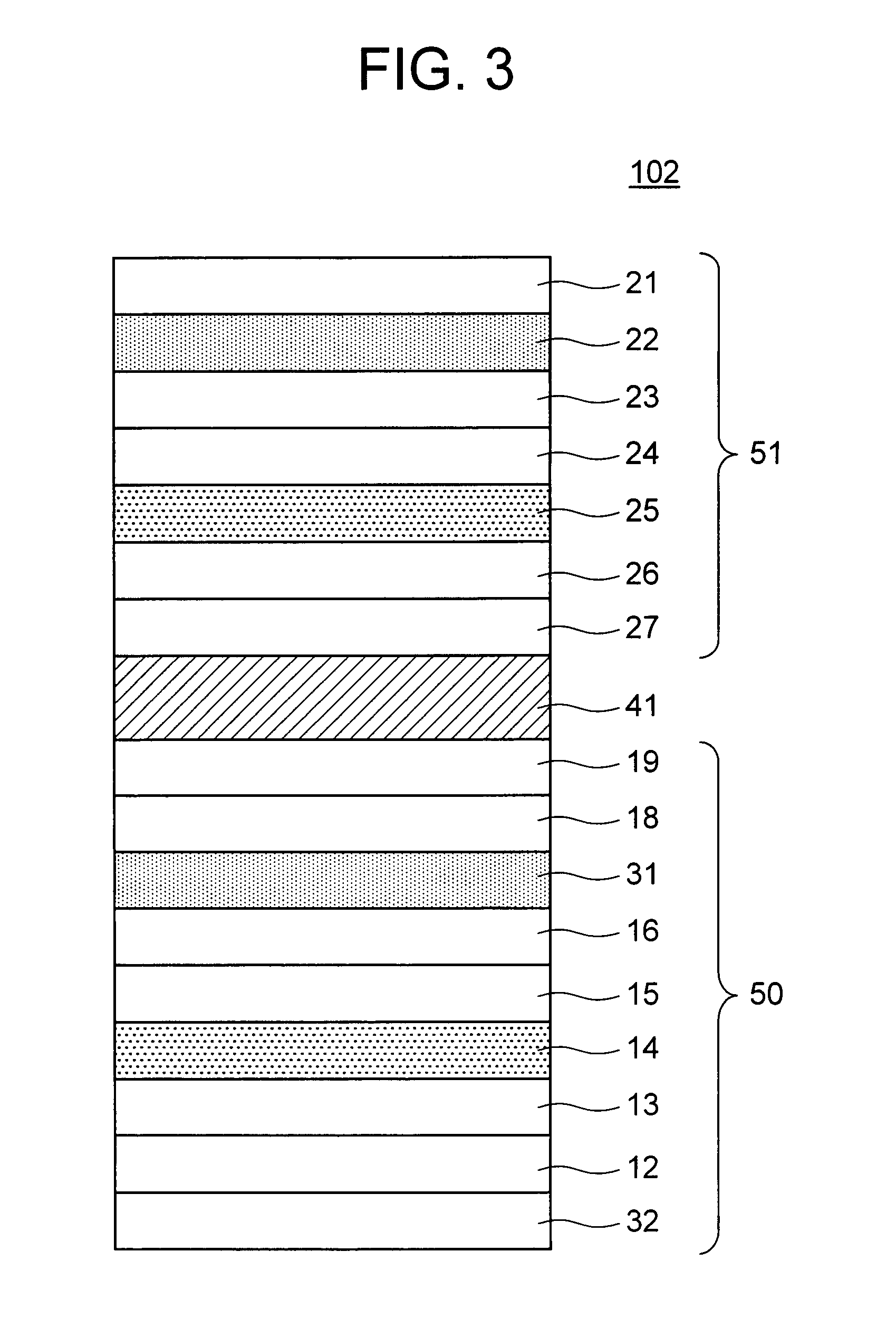
[0075] Optical disks of Example 3 were prepared by forming optical disks similar to those of Example 2 except for using a 15 nm-thick film containing Nb2O5 at 70 mol % and Al2O3 at 30 mol % for the second dielectric film 16 prepared in Example 1. The relationship of items same as those of Table 7 was examined. Table 8 below shows some of the obtained results.
TABLE 8ThirdRefractivePresence ordielectricindexTransmittanceNumber ofabsence offilm 18differencefactor (%)candidatessulfurationZnS—SiO2093.22AbsentGeN0.296.86AbsentSiN0.2597.19AbsentAl2O30.498.214AbsentAl2O3—HfO20.4598.618AbsentHfO20.599.018AbsentAl2O3—SiO20.5599.219AbsentHfO2—SiO20.6100.220AbsentSiO20.7101.422Absent
[0076] By paying attention to the refractive index difference, the transmission factor of light and the number of candidates in Tables 7 and 8, it was found that the transmission factor of light rises and the number of candidates increases as the refractive index difference increases. In other words, it is possibl...
PUM
| Property | Measurement | Unit |
|---|---|---|
| wavelength | aaaaa | aaaaa |
| wavelength | aaaaa | aaaaa |
| thickness | aaaaa | aaaaa |
Abstract
Description
Claims
Application Information
 - Generate Ideas
- Intellectual Property
- Life Sciences
- Materials
- Tech Scout
- Unparalleled Data Quality
- Higher Quality Content
- 60% Fewer Hallucinations
Browse by: Latest US Patents, China's latest patents, Technical Efficacy Thesaurus, Application Domain, Technology Topic, Popular Technical Reports.
© 2025 PatSnap. All rights reserved.Legal|Privacy policy|Modern Slavery Act Transparency Statement|Sitemap|About US| Contact US: help@patsnap.com


