Display device and manufacturing method of the same
a technology of a display device and a manufacturing method, applied in the field of display devices, can solve problems such as properties changes, and achieve the effects of favorable performance, favorable light-blocking properties, and favorable performan
- Summary
- Abstract
- Description
- Claims
- Application Information
AI Technical Summary
Benefits of technology
Problems solved by technology
Method used
Image
Examples
embodiment mode 1
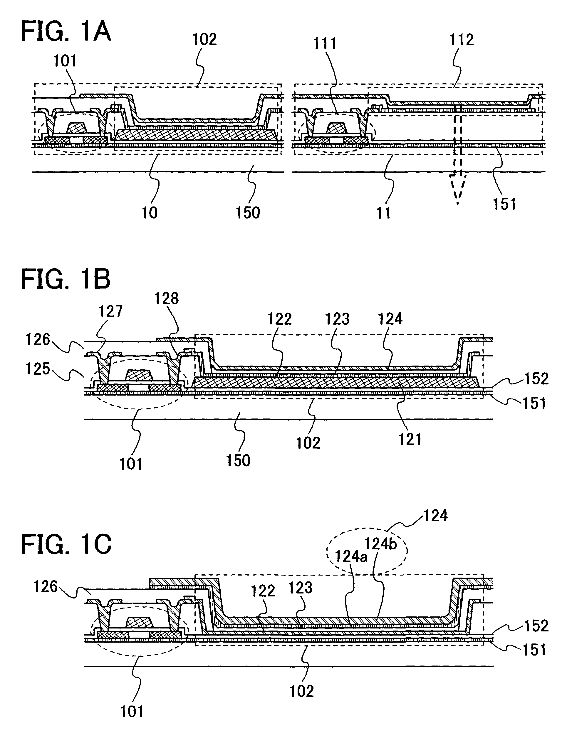
[0034]FIG. 1A is a view showing a mode of implementing the present invention. In a region indicated by a dotted frame 10, a TFT 101 and a monitoring element portion including a monitoring element 102 which is a light emitting element and the like are provided. In a region indicated by a dotted frame 11, a TFT 111 and a pixel portion including a light emitting element 112 and the like are provided. These are formed over a substrate 150 which is formed using a material having a light-transmitting property, such as glass or plastic. A base film 151, a gate insulating film 152, and the like may be formed over the substrate 150. Furthermore, although the peripheral circuit 200 which is shown in FIG. 2A for the related art is not shown in FIGS. 1A to 1C, it may be provided in the vicinity of the monitoring element portion or the pixel portion.
[0035]FIG. 1B is an enlarged view of the monitoring element portion shown in FIG. 1A. Concurrently with forming the TFT 101, a light-blocking layer...
embodiment mode 2
[0041]FIGS. 3A to 3D show a different mode of the structure shown in FIG. 1B. In the top emission case, the pixel electrode formed using a material having reflectivity or a light-blocking property and the counter electrode including the light-blocking layer surround the light emitting layer in the horizontal direction as well (as shown in FIG. 1C). In the bottom emission case, however, the structure shown in FIG. 1B may not sufficiently prevent leak light since only the pixel electrode formed using a material having a light transmitting property surrounds the light emitting layer in the horizontal direction.
[0042] As the countermeasure against this, there is a method in which a structure using a material having a light-blocking property is formed in the horizontal direction. Hereinafter, the method will be described in detail referring to FIGS. 3A to 3D.
[0043]FIGS. 3A to 3C show structures of the monitoring element portion seen from the top, and a cross-sectional structure along li...
embodiment 1
[0056] Formation of a display device having the structure of the present invention will be described with reference to drawings. Here, each step will be described in order, using FIGS. 4A and 4B. Although FIGS. 4A and 4B show a cross-section of only a monitoring element portion, TFTs, a wiring and the like constituting a peripheral circuit may be formed concurrently with a step of forming a TFT included in the monitoring element portion, and a pixel portion may be formed in the same way; therefore, they are not illustrated here.
[0057]FIG. 4A shows a cross-sectional view of a bottom emission display device, and FIG. 4B shows a cross-sectional view of a top emission display device. The same reference numerals are used for the structures common to the two views. Hereinafter, the description will be made with reference to the two views.
[0058] As a substrate 401 having an insulating surface, a glass substrate, a quartz substrate, or the like can be used. A substrate formed of a synthet...
PUM
 Abstract
Description
Claims
Application Information
 - R&D
- Intellectual Property
- Life Sciences
- Materials
- Tech Scout
- Unparalleled Data Quality
- Higher Quality Content
- 60% Fewer Hallucinations
Browse by: Latest US Patents, China's latest patents, Technical Efficacy Thesaurus, Application Domain, Technology Topic, Popular Technical Reports.
© 2025 PatSnap. All rights reserved.Legal|Privacy policy|Modern Slavery Act Transparency Statement|Sitemap|About US| Contact US: help@patsnap.com


