
Apparatus and method for processing image signal without requiring high memory bandwidth

a technology of image signal and memory bandwidth, applied in the field of image signal processing apparatus and method, can solve the problems of limited memory bandwidth and exacerbated image signal processing delay, and achieve the effects of maintaining or magnifying and reducing the image size of the input image signal

Active Publication Date: 2007-07-12
SAMSUNG ELECTRONICS CO LTD
View PDF3 Cites 49 Cited by
  • Summary
  • Abstract
  • Description
  • Claims
  • Application Information

AI Technical Summary

Benefits of technology

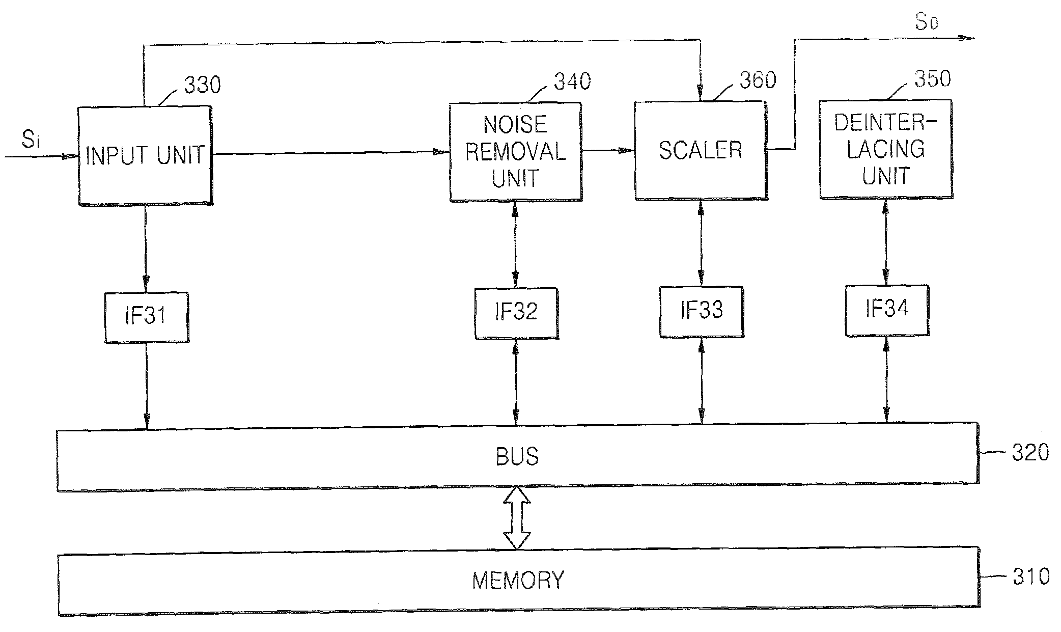
[0015]According to an exemplary embodiment of the present invention, there is provided an image signal processor for processing an input image signal to output an output image signal. The image signal processor includes an input unit receiving the input image signal, a noise removal unit removing noise from the input image signal, and a scaler reducing, maintaining or magnifying the image size of an image signal input thereto. The scaler directly receives the input image signal from the input unit or the noise removal unit in response to a route control signal, reduces the image size of the input image signal when the image size of the input image signal is larger than the image size of the output image signal and stores the image signal with a reduced image size in a memory. The scaler maintains or magnifies the image size of the image signal stored in the memory and outputs the image signal with a maintained or magnified image size as the output image signal.
[0016]According to an exemplary embodiment of the present invention, there is provided a method of processing a image signal. The method includes the steps of directly transmitting an input image signal from an input unit or a noise removal unit to a scaler when the image size of the input image signal is larger than the image size of the output image signal, reducing the image size of the input image signal directly transmitted to the scaler to correspond to the image size of the output image signal to generate a reduced image signal and storing the reduced image signal in the memory, and reading the reduced image signal from the memory and outputting the read image signal as the output image signal.
[0017]According to an exemplary embodiment of the present invention, there is provided a image signal processor for processing a main input image signal and a sub input image signal for forming a PIP image. The image signal processor includes a first input unit receiving the main input image signal, a second input unit receiving the sub input image signal, a noise removal unit removing noise from an image signal input thereto, a deinterlacing unit deinterlacing an image signal input thereto, first and second scalers scaling the image sizes of the main and sub input image signals, first and second multiplexers controlling routes of the main and sub input image signals, and an output multiplexer receiving a main output image signal and a sub output image signal output from the first or second scaler. The main input image signal and the sub input image signal may be directly transmitted to the noise removal unit or the first and second scalers without passing through a memory. The first or second scaler may reduce the image size of the main input image signal or the sub input image signal to correspond to the image size of the main output image signal or the sub output image signal and store the image signal with a reduced image size in the memory.

Problems solved by technology

When processing a high definition (HD) image signal having a large data capacity, the experienced image signal processing delay is exacerbated.
However, this becomes a problem in image signal processing because memory bandwidth is limited.

Method used


Image

  • Apparatus and method for processing image signal without requiring high memory bandwidth
  • Apparatus and method for processing image signal without requiring high memory bandwidth
  • Apparatus and method for processing image signal without requiring high memory bandwidth

Examples


Embodiment Construction

[0025]The present invention will now be described more fully with reference to the accompanying drawings, in which exemplary embodiments of the invention are shown. The invention may, however, be embodied in many different forms and should not be construed as being limited to the embodiments set forth herein.

[0026]FIG. 3 is a block diagram of an image signal processor according to an exemplary embodiment of the present invention. The image signal processor includes a memory 310, a bus 320, a plurality of interface units IF31, IF32, IF33 and IF34, an input unit 330, a noise removal unit 340, a deinterlacing unit 350 and a scaler 360. The image signal processor receives an input image signal Si, processes the input image signal Si and outputs an output image signal Sc.

[0027]The input image signal Si input to the input unit 330 can be directly transmitted to the noise removal unit 340 or the scaler 360. Alternatively the input image signal Si can be transmitted to the memory 310 via th...


PUM


Abstract

An image signal processor for processing an input image signal to output an output image signal includes an input unit receiving the input image signal, a noise removal unit removing noise from the input image signal, and a scaler reducing, maintaining or magnifying the image size of the input image signal. The scaler directly receives the input image signal from the input unit or the noise removal unit in response to a route control signal, reduces the image size of the input image signal when the image size of the input image signal is larger than the image size of the output image signal and stores the image signal with a reduced image size in a memory. The scaler maintains or magnifies the image size of the image signal stored in the memory and outputs the image signal with a maintained or magnified image size as the output image signal.

Description

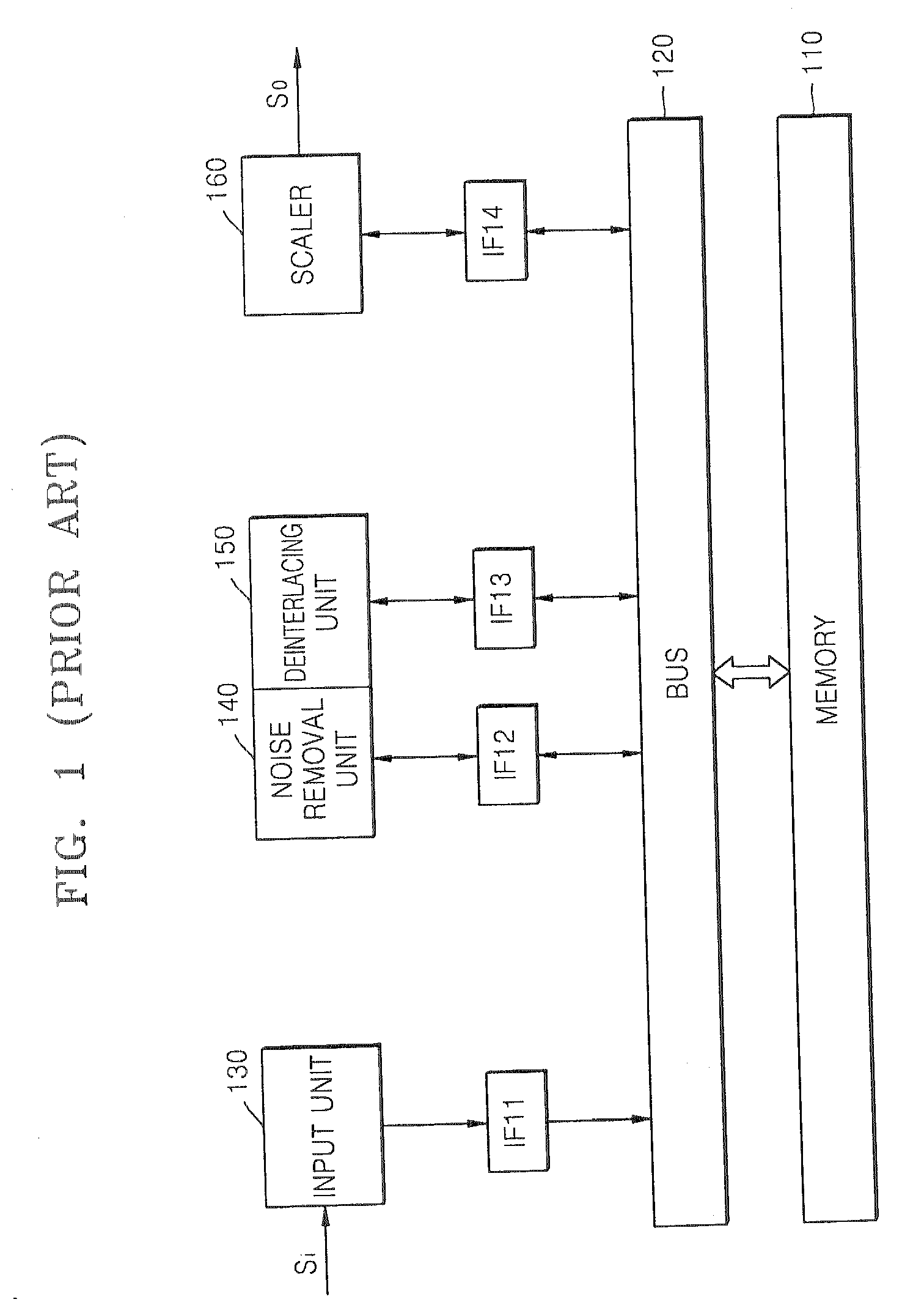
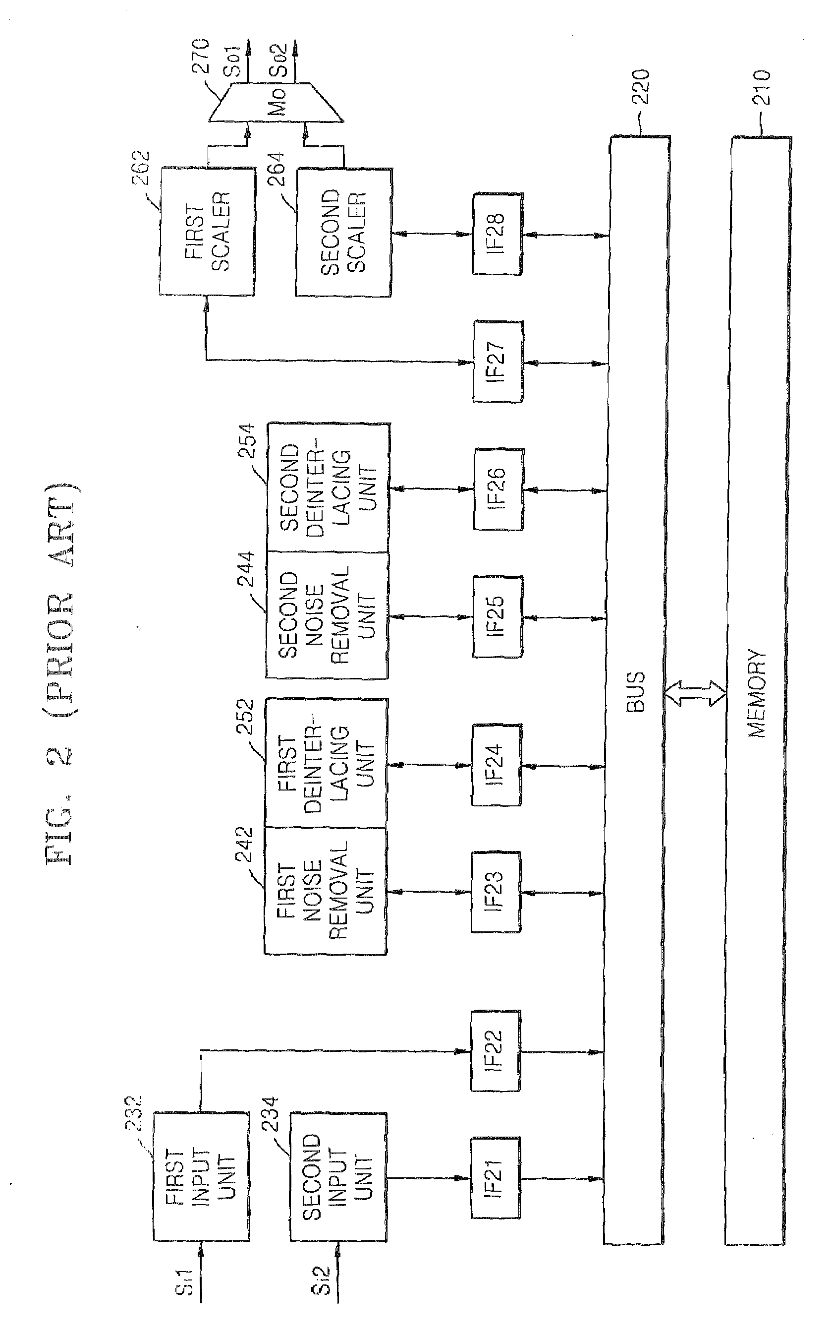
CROSS-REFERENCE TO RELATED PATENT APPLICATION[0001]This application claims priority to Korean Patent Application No. 10-2006-0002675, filed on Jan. 10, 2006, in the Korean Intellectual Property Office, the disclosure of which is incorporated by reference herein in its entirety.BACKGROUND OF THE INVENTION[0002]1. Technical Field[0003]The present disclosure relates to an image signal processing apparatus and method, and more particularly, to a image signal processing apparatus and method which minimizes the number of memory accesses and does not require a high memory bandwidth.[0004]2. Discussion of the Related Art[0005]An image signal captured by a video camera or a camcorder is transmitted to a display device such as a digital TV via an image signal processor. The image signal processor removes noise from the image signal, deinterlaces the image signal when the image signal is an interlaced image signal, and scales the image signal when necessary.[0006]FIG. 1 is a block diagram of a...

Claims


Application Information

Patent Timeline
IPC IPC(8): G06K15/02
CPCG06T3/40H04N5/21H04N21/440263H04N7/012H04N21/4316H04N5/45E05B1/003E05B65/0811E05Y2900/148
Inventor CHOI, HO-YOUN
Owner SAMSUNG ELECTRONICS CO LTD
Learn More