
Curved optical waveguide and optical device

a waveguide and optical technology, applied in the field of curved optical waveguides and optical devices, can solve the problems of inability to provide an optimum axial deviation amount in a wide wavelength range due to wavelength dependence, difficulty in forming infinite gaps in high yield, fluctuation in loss, etc., and achieves low loss, small variation upon production, and high yield.

Inactive Publication Date: 2007-07-05
HITACHI CHEM CO LTD
View PDF4 Cites 9 Cited by
  • Summary
  • Abstract
  • Description
  • Claims
  • Application Information

AI Technical Summary

Benefits of technology

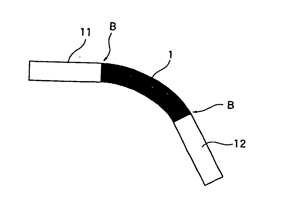
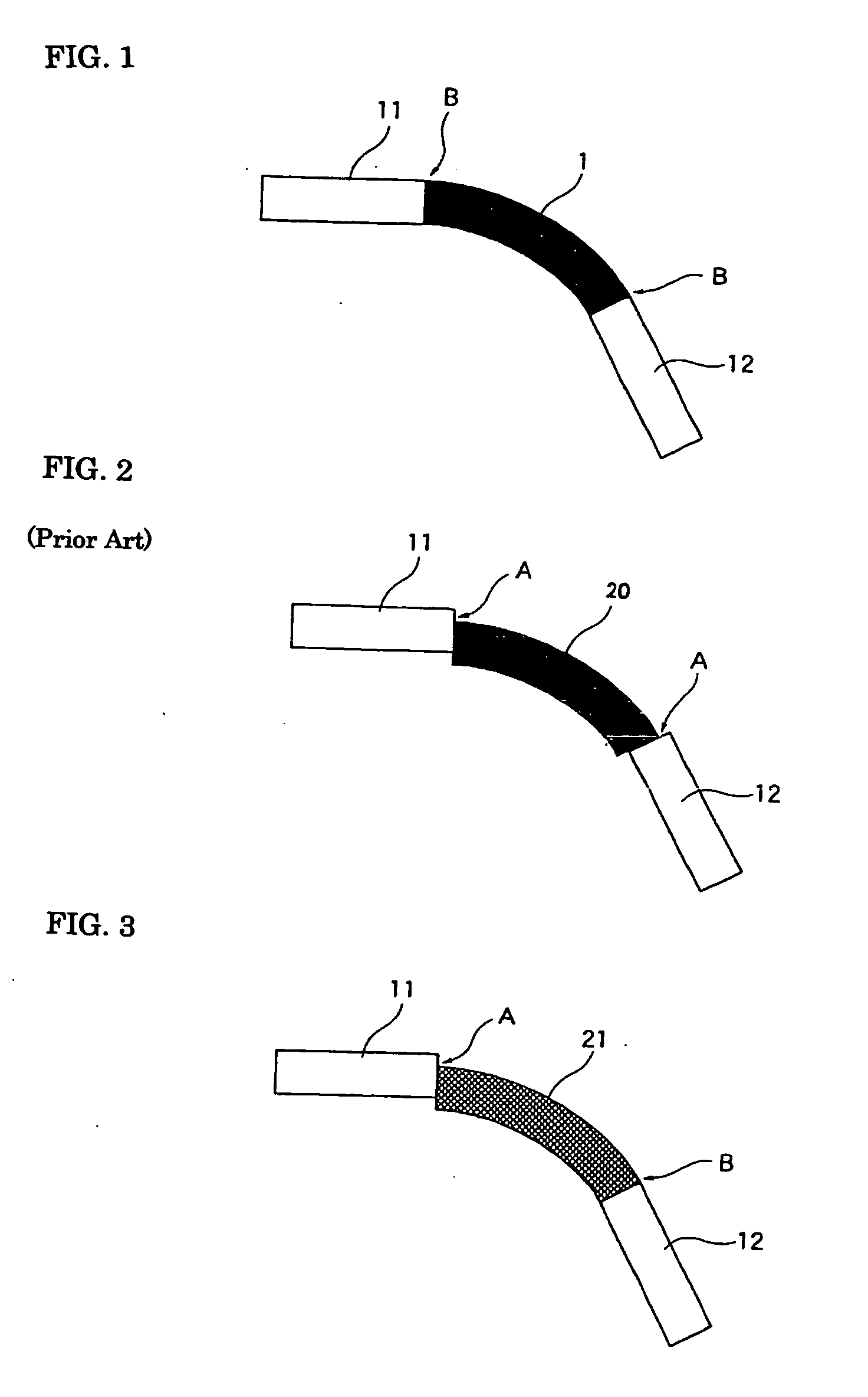
[0015] An object of the present invention is to provide a curved optical waveguide that can be suitably used in the case where such optical waveguides having different properties as described above are connected under such circumstances.

Problems solved by technology

However, it is extremely difficult to form an infinitesimal gap in high yield and to widen the gap from an infinitesimal one gradually owing to restrictions upon production.
Since an axial deviation amount depends on a relative refractive index between a core and a clad, the dimensions of the core, and a wavelength, the fact that fluctuations in the refractive index and the dimensions of the core due to variations upon production are responsible for a fluctuation in loss has been a problem.
The incapability to provide an optimum axial deviation amount in a wide wavelength range due to wavelength dependence has been also a problem.
Accordingly, it has been difficult to establish a symmetric branching ratio (1:1).
In addition, an axial deviation amount and asymmetry are different at different wavelengths, so it has been difficult to keep a branching ratio constant in a wide wavelength range.
However, the approach involves a disadvantage in that an excessive loss occurs at a junction of the straight line-optical waveguide with a curved optical waveguide and a disadvantage in that the total length of an optical waveguide increases so that the size of the optical waveguide increases.
As a result, an optical loss occurs.
Accordingly, it is difficult to provide an optimum axial deviation structure owing to factors such as a variation upon production.
In general, the absence of an axial deviation structure is preferable because otherwise a problem arises in that an optical loss occurs.
The incapability to provide an optimum axial deviation amount in a wide wavelength range due to wavelength dependence has been also a problem.

Method used


Image

  • Curved optical waveguide and optical device
  • Curved optical waveguide and optical device
  • Curved optical waveguide and optical device

Examples


example 1

[0124] Evaluation about an excessive loss at a curved part in the present invention was performed as described below (input wavelengths of 1.31 μm and 1.55 μm).

[0125] The optical waveguides 1 to 4 of the first aspect of the invention each having a curve expressed by the function of the equation [II] as a central line were disposed by connecting as shown in FIG. 21. At this time, a length in a z-axis direction was 2.6775 mm, and a length in the direction perpendicular to a z-axis was 0.125 mm. To be specific, the resultant was enlarged or reduced in a z direction or x direction in such a manner that the equation [II] would be expressed in the form of the following equation [X]. Thus, the shape of an optical waveguide was obtained.

Trajectory of the central line of an optical waveguide:

x / height=z / length−sin [π(z / length)] / π  [X]

where height=0.125 mm and length=2.6775 mm.

[0126] No offset was provided for every junction between middle and intervening sections. In addition, the optic...

example 2

[0133] Next, the excessive loss of a 1×8 splitter having a constitution shown in FIG. 22 was calculated. In the figure, the optical waveguide of the present invention having a curve represented by the function of the equation [II] was used in a section 1 expressed by a solid line, the optical waveguides of the present invention each having a curve represented by the function of the equation [III] were used in sections 2 to 10 expressed by solid lines, curved optical waveguides each shown in FIG. 6 and straight line-optical waveguides were used in sections 51 to 64 expressed by dotted lines, and multi-mode optical waveguides were used in sections 34 to 40. When the optical waveguides of the present invention were used for connection, an average excessive loss was −9.53 dB (for an input wavelength of 1.31 μm) or −9.76 dB (for an input wavelength of 1.55 μm). Next, for comparison, the excessive loss of a 1×8 splitter having a constitution similar to that shown in FIG. 22 was calculated...

example 3

[0136] An optical splitter having a curved optical waveguide having a schematic structure shown in FIG. 22 was produced by using the following materials.

Core: OPI-N3205 manufactured by Hitachi Chemical Co., Ltd.

Clad: OPI-N1005 manufactured by Hitachi Chemical Co., Ltd.

[0137] Production method; an organic zirconium chelate was applied by means of a spin coating method to a silicon wafer in which V grooves had been formed in such a manner that the chelate would have a thickness of 100 angstroms after drying. After the resultant had been dried, a polyimide resin free of fluorine was applied to the resultant in such a manner that the resin would have a thickness of 0.3 μm after drying. After the resultant had been dried, a lower clad layer (8 μm) and a core layer (6.5 μm) each composed of a polyimide resin containing fluorine were formed. Next, a silicon-containing resist was applied on the core layer to have a thickness of 0.5 μm, and was dried. The resultant was subjected to expo...


PUM


Abstract

A curved optical waveguide comprising a core and a clad, characterized in that: the core shape of the curved optical waveguide has no reversal of a curvature on a halfway; and curvatures at both ends of the curved optical waveguide gradually approach zero. A curved optical waveguide comprising a core and a clad, characterized in that: the core shape of the curved optical waveguide has no reversal of a curvature on a halfway; a curvature at one end of the curved optical waveguide gradually approaches zero; and a radius of curvature at other end is finite. An optical waveguide comprising such a curved optical waveguide and an optical waveguide having a different core shape optically connected with the former, and an optical device using such a curved optical waveguide.

Description

TECHNICAL FIELD [0001] The present invention relates to a curved optical waveguide and an optical device using the same. BACKGROUND ART [0002] There has been an abruptly growing demand on information transmission in association with a recent widespread use of personal computers and the Internet, so optical transmission with a high transmission rate has become widespread. An optical waveguide has been used as an optical interconnection in such optical transmission. [0003] When a 1×2 branching section is constituted, for example, in the case where a branching and coupling device for optical transmission is constituted, in junctions where two curved optical waveguides connect with a branching section (outlets of a branching section of the optical waveguide), gradually widening a gap between both the curved optical waveguides from an infinitesimal one is an ideal way effective in reducing an excessive loss at a branching section. However, it is extremely difficult to form an infinitesim...

Claims


Application Information

Patent Timeline
Patent Type & Authority Applications(United States)
IPC IPC(8): G02B6/26G02B6/42G02B6/125G02B6/30
CPCG02B6/30G02B6/125
Inventor MIYADERA, NOBUOYAMAMOTO, REI
Owner HITACHI CHEM CO LTD
Learn More