
Thermal sensing method and system

a technology of temperature sensor and integrated circuit, applied in the field of temperature sensor, can solve the problems of cmos transistor failure, time-consuming and costly calibration of temperature sensor,

Inactive Publication Date: 2007-06-28
BOERSTLER DAVID WILLIAM +1
View PDF19 Cites 15 Cited by
  • Summary
  • Abstract
  • Description
  • Claims
  • Application Information

AI Technical Summary

Benefits of technology

"The present invention provides a method for identifying the hottest area of an integrated circuit. This is done by measuring the temperature of two different areas of the chip and comparing them. If there is a significant difference in the readings, an error condition is indicated. This method can help improve the performance and reliability of the integrated circuit."

Problems solved by technology

If this heat is neither properly dissipated nor otherwise accounted or compensated for, the CMOS transistor can experience degradation leading to CMOS transistor failure.
Calibration of temperature sensors can be time intensive and costly.
Furthermore, the measurement of heat by the temperature sensors in ICs, such as an IC manufactured using the silicon on insulator (SOI) approach, has proven problematic, due to such factors as thermal isolation of CMOS transistors in the chip.

Method used


Image

  • Thermal sensing method and system
  • Thermal sensing method and system
  • Thermal sensing method and system

Examples


Embodiment Construction

[0011] In the following discussion, numerous specific details are set forth to provide a thorough understanding of the present invention. However, those skilled in the art will appreciate that the present invention may be practiced without such specific details. In other instances, well-known elements have been illustrated in schematic or block diagram form in order not to obscure the present invention in unnecessary detail. Additionally, for the most part, details concerning network communications, electromagnetic signaling techniques, and the like, have been omitted inasmuch as such details are not considered necessary to obtain a complete understanding of the present invention, and are considered to be within the understanding of persons of ordinary skill in the relevant art.

[0012] It is further noted that, unless indicated otherwise, all functions described herein may be performed in either hardware or software, or some combination thereof In a preferred embodiment, however, th...


PUM

PropertyMeasurementUnit
hot areaaaaaaaaaaa
areaaaaaaaaaaa
temperatureaaaaaaaaaa

Abstract

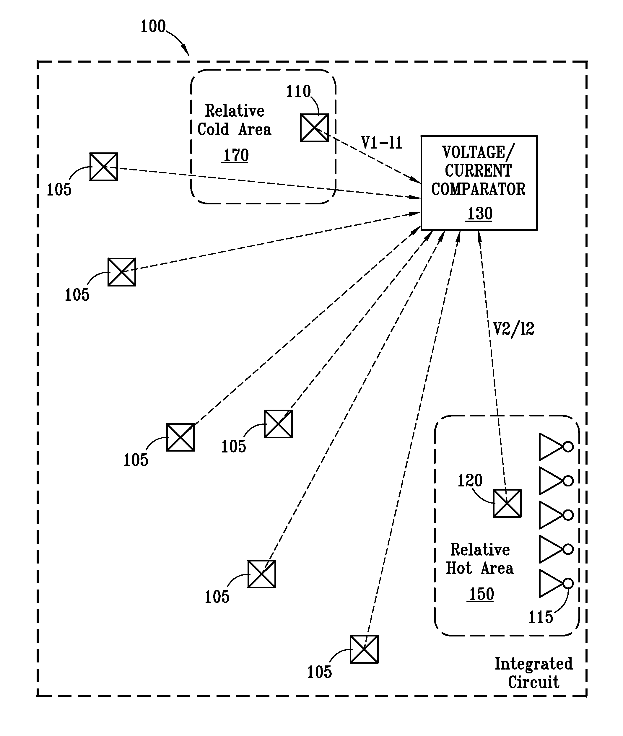
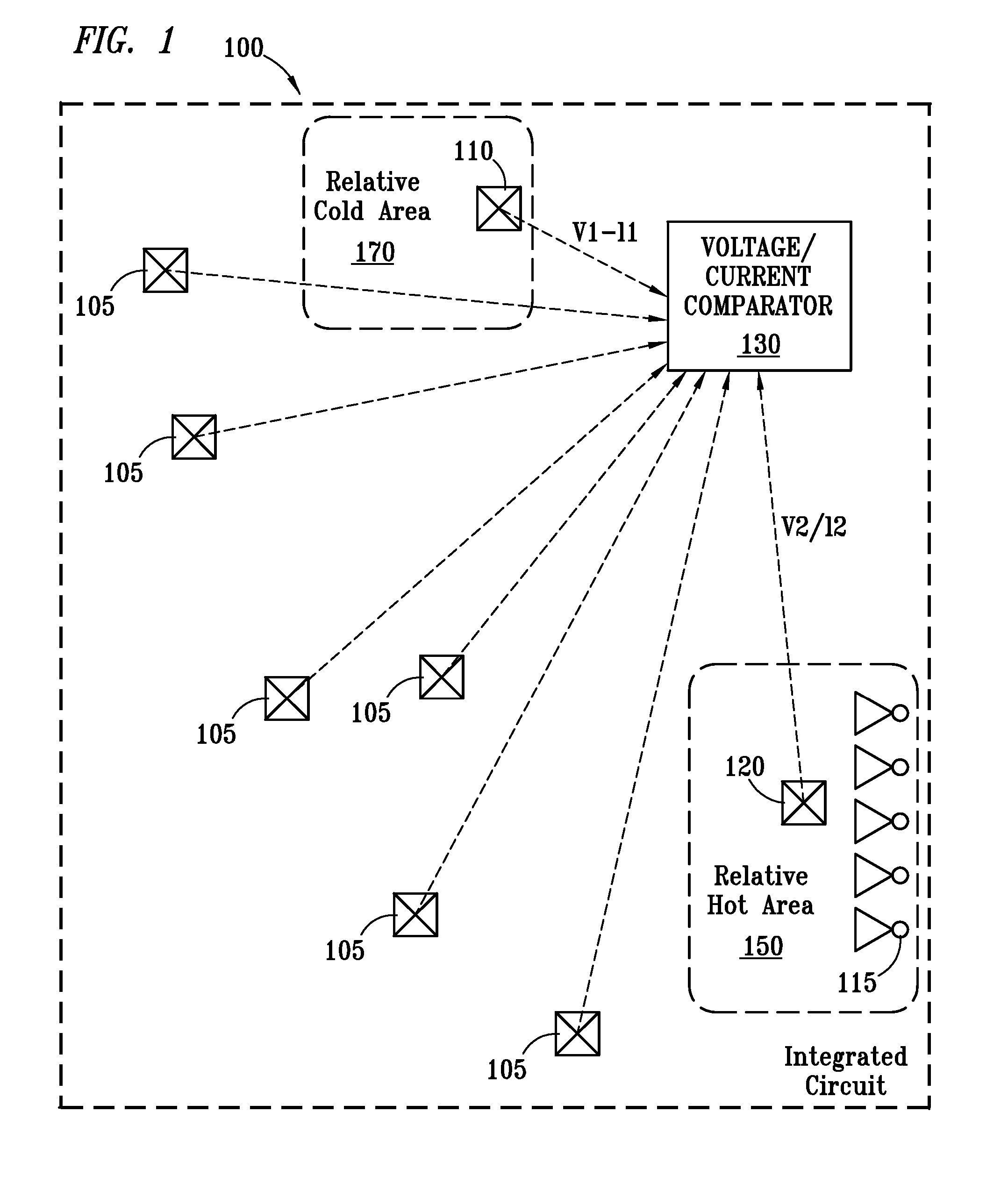
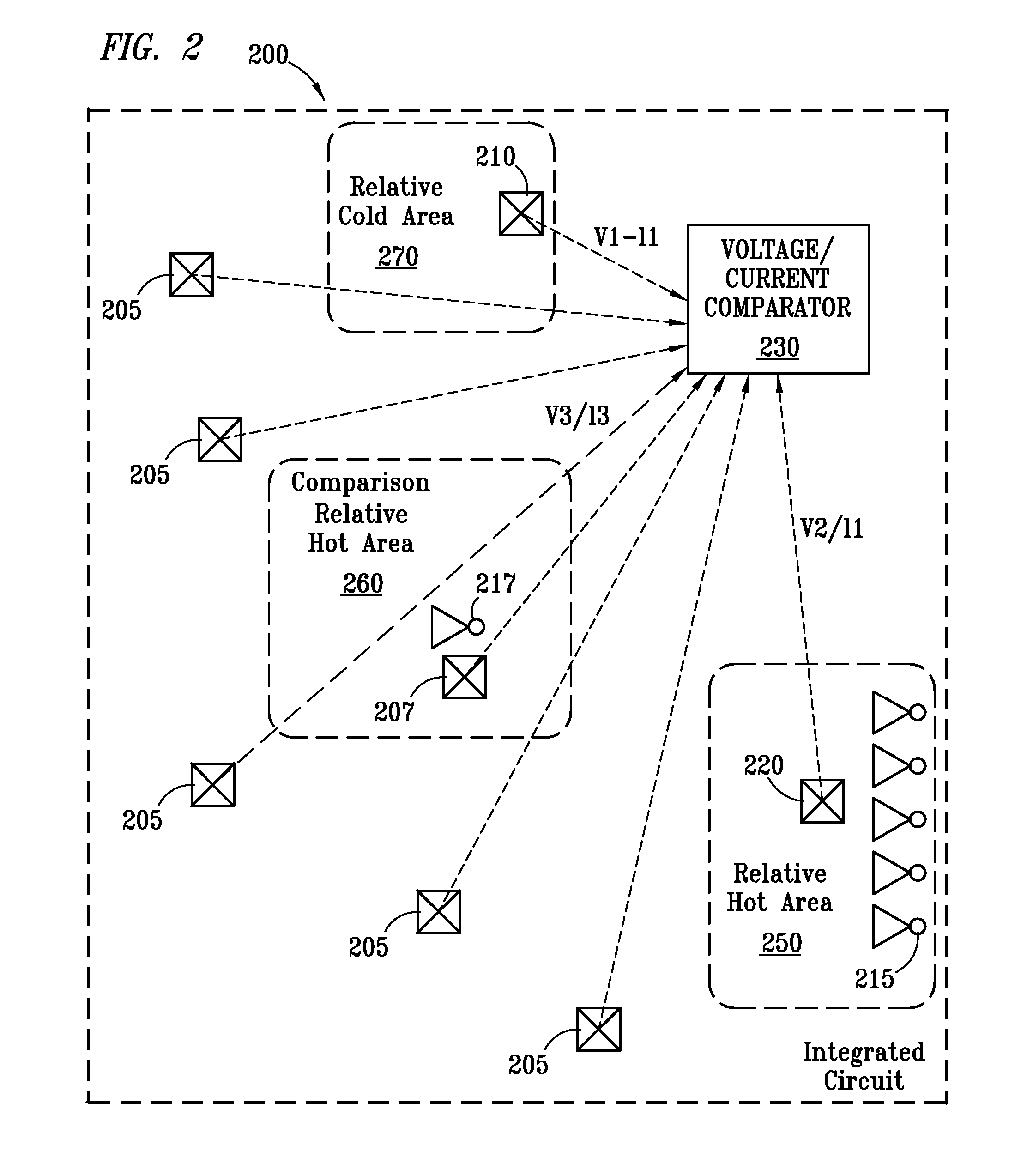
The present invention provides a method for determining a hot area of an integrated circuit. A first temperature sensor in a first area of a chip is read, the chip comprising a plurality of chip areas, wherein the first area is a comparison area. The comparison area comprises at least one I / O device that is controlled to simulate other functional I / O devices on the chip. A second temperature sensor in a second area of a chip is read. The readings of the first temperature sensor and the second temperature sensor are compared. If the difference between the first temperature reading and the second temperature reading exceeds a threshold, a first error condition is indicated.

Description

CROSS-REFERENCE TO RELATED APPLICATIONS [0001] This application is a division of, and claims the benefit of the filing date of, co-pending U.S. patent application Ser. No. 10 / 606,586 entitled THERMAL SENSING METHOD AND SYSTEM, filed Jun. 26,2003.TECHNICAL FIELD [0002] The invention relates generally to thermal sensing and, more particularly, to thermal sensing in an integrated circuit. BACKGROUND [0003] A complementary metal-oxide semiconductor (CMOS) is one type of transistor used in an integrated circuit (IC). CMOS transistors generate heat when switching from an off state to an on state, or from an on state to an off state, within the IC. If this heat is neither properly dissipated nor otherwise accounted or compensated for, the CMOS transistor can experience degradation leading to CMOS transistor failure. [0004] Silicon on insulator (SOI) technology can be employed in CMOS fabrication. Generally, SOI is a manufacturing technique in which devices are fabricated on top of a relati...

Claims


Application Information

Patent Timeline
Patent Type & Authority Applications(United States)
IPC IPC(8): G01K1/08G01K1/02G01K3/14G01K7/01H01L27/02H02H5/04
CPCG01K1/026G01K3/14G01K7/01H01L27/0248
Inventor BOERSTLER, DAVID WILLIAMYOSHIDA, MUNEHIRO
Owner BOERSTLER DAVID WILLIAM
Learn More