
Semiconductor integrated circuit device, method of testing the same, database for design of the same and method of designing the same

a technology of integrated circuit devices and semiconductors, applied in the field can solve the problems of extremely large peak power consumption, high cost of integrated circuit devices, and very large momentary power consumption during test, so as to suppress the increase of the time of using testers and reduce the peak power consumption

Inactive Publication Date: 2007-05-10
PANASONIC CORP
View PDF20 Cites 8 Cited by
  • Summary
  • Abstract
  • Description
  • Claims
  • Application Information

AI Technical Summary

Benefits of technology

"The invention aims to reduce peak power consumption during a scan test of an integrated circuit device. This is achieved by providing means for dispersing the operation timing of circuit elements in the device, while preventing changes in the internal state of the logic circuits during the shift operation of the scan test. The first integrated circuit device of the invention includes multiple logic circuits and flip-flop circuits connected in a scan test circuit. A scan test is conducted by repeating a holding operation for fixing an output signal from each flip-flop circuit, a shift operation for sending a scan test signal and a data signal to the logic circuits, a hold releasing operation for releasing the output signal after the shift operation, and a capture operation for capturing the output signal. The second integrated circuit device of the invention includes first and second circuits, a clock supply part for supplying a clock signal to the first and second circuits, a clock inverting part for inverting the clock signal, and an output switching circuit for selectively outputting the inverted clock signal or the original clock signal. The methods described in the patent text can be used to suppress peak power consumption during the scan test and hold the output signal in a fixed state during the shift operation."

Problems solved by technology

This is because, when the tester is used for a long period of time, the cost of the integrated circuit device ultimately becomes high due to high running cost of the tester.
When a large number of cores are operated in a short period of time as in the aforementioned scan test of the integrated circuit device, however, the momentary power consumption (peak power consumption) during the test can be very large.
Particularly, since a large number of and a variety of circuits are recently packed in one chip of an integrated circuit device such as a system LSI, the peak power consumption is estimated to be extremely large.
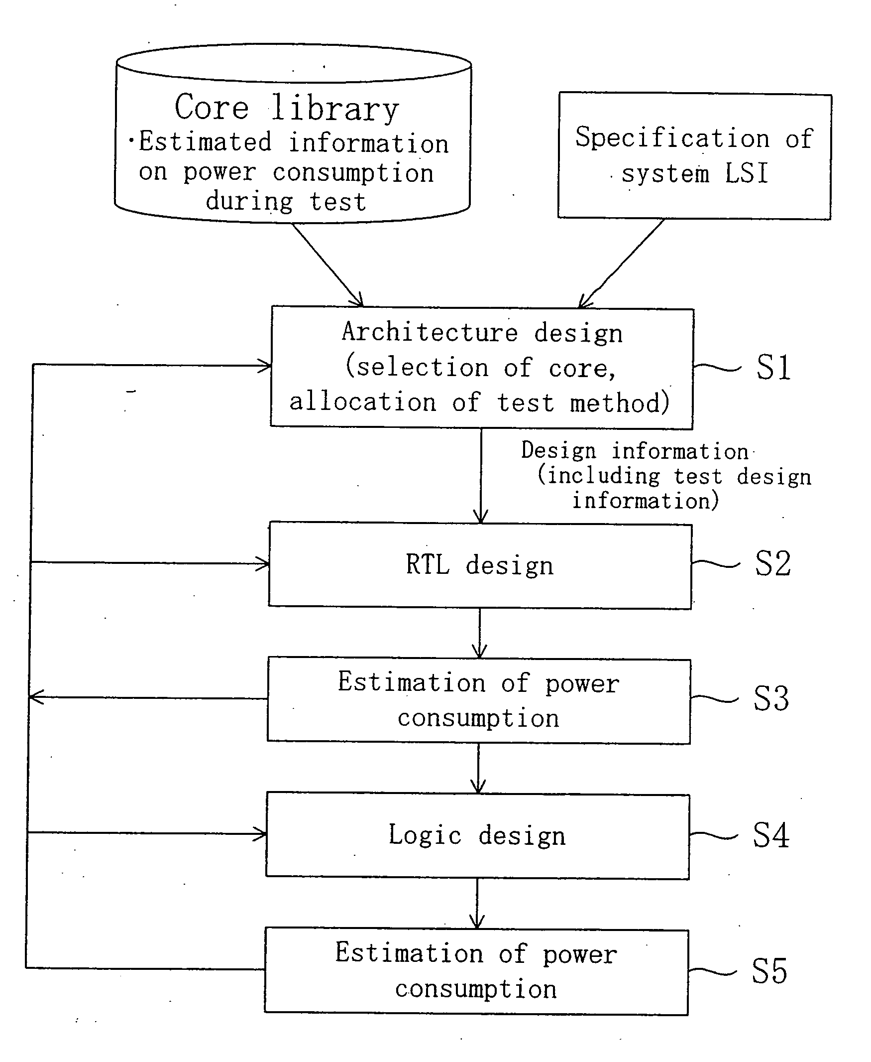
Although power supply is generally designed with respect to power consumption during general use of a device, the power supply design does not take the increase of peak power consumption during the test into consideration.
In general use, there is substantially no chance that all the circuits included in an integrated circuit device are simultaneously operated, and hence, the peak power consumption during general use is not very large.
As a result, an integrated circuit device designed without considering the peak power consumption during the test cannot be normally operated in the scan test or can be damaged by the test.

Method used


Image

  • Semiconductor integrated circuit device, method of testing the same, database for design of the same and method of designing the same
  • Semiconductor integrated circuit device, method of testing the same, database for design of the same and method of designing the same
  • Semiconductor integrated circuit device, method of testing the same, database for design of the same and method of designing the same

Examples


embodiment 1

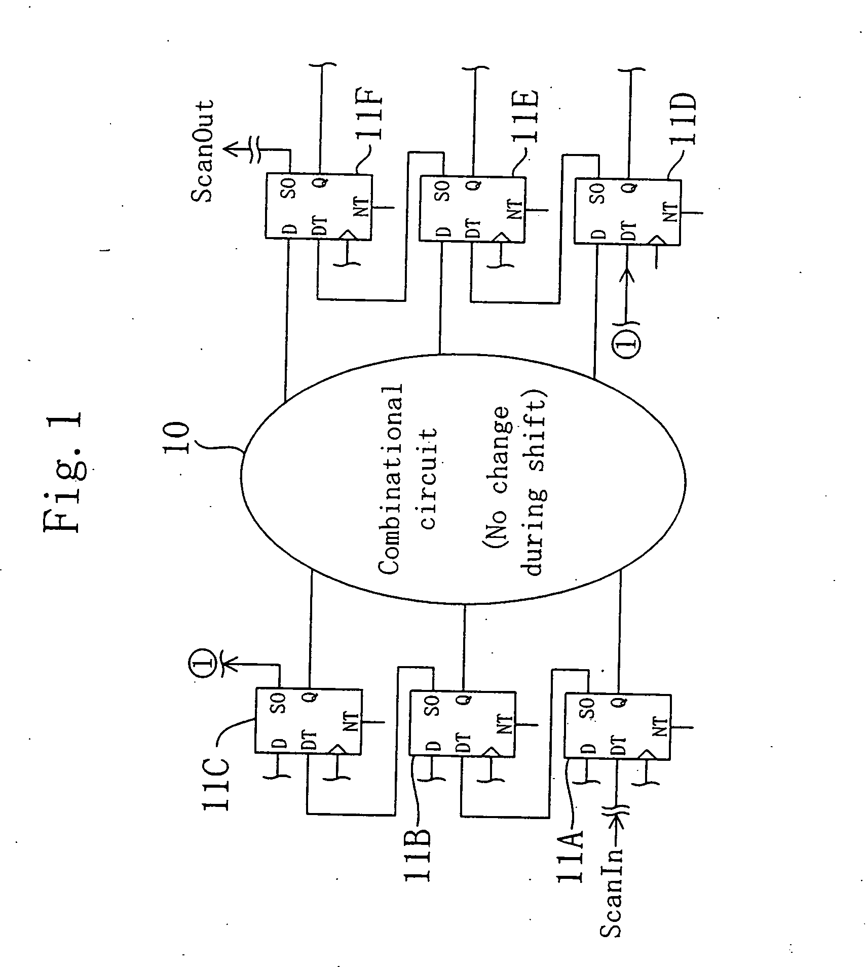
[0061]FIG. 1 is a diagram for showing part of a system LSI, that is, an integrated circuit device according to Embodiment 1. As is shown in FIG. 1, the system LSI includes a combinational circuit 10, that is, one logic circuit within the system LSI, and flip-flop circuits 11A through 11F disposed between and connected to the combinational circuits 10. Although merely one combinational circuit 10 is shown in FIG. 1, flip-flop circuits within the system LSI are actually used as scan test circuits for testing combinational circuits including a large number of elements of the system LSI. As the flip-flop circuits 11A through 11F, flip-flops provided for general use are used as much as possible.

[0062] The system LSI also includes a circuit not applicable to the scan test, and such a circuit is tested by another test method.

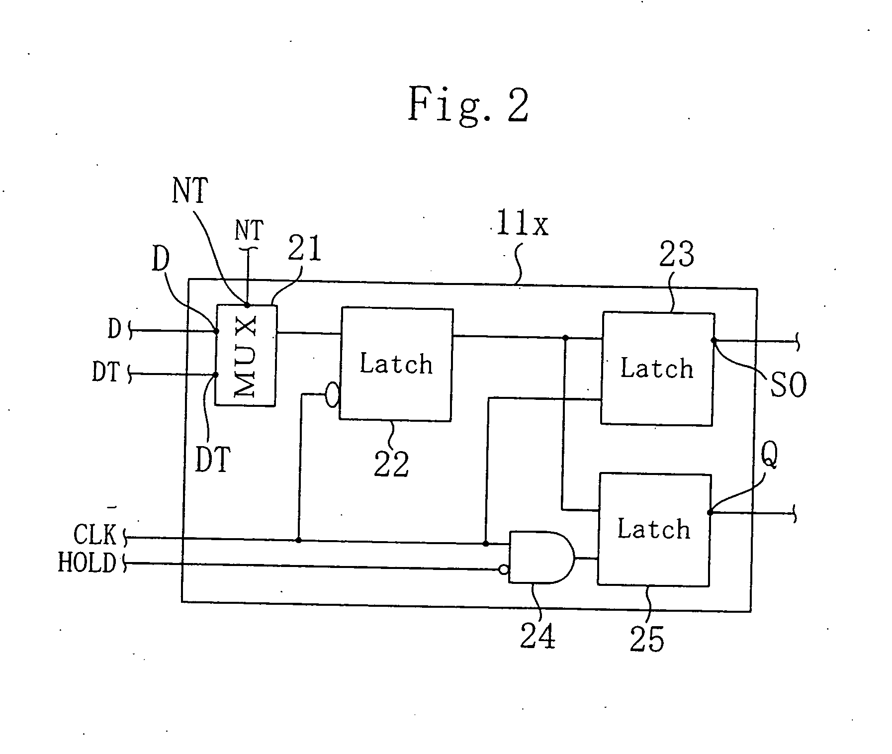
[0063] Each flip-flop circuit 11 has a terminal D for bringing in a data signal D, a terminal DT for bringing in a scan test signal DT, a clock terminal for bringing...

embodiment 2

[0078] In Embodiment 2, scan test methods performed by utilizing the configurations of the flip-flop circuit described as the specific examples in Embodiment 1 will be described.

[0079]—First Example of Scan Test Method—

[0080]FIG. 4(a) is a circuit diagram for showing part of a system LSI to be tested by a first example of the scan test method, and FIG. 4(b) is a diagram for showing change of the test mode. In this example, the flip-flop circuit 11x (shown in FIG. 2) described as the first example of Embodiment 1 is used.

[0081] First, as is shown in FIG. 4(a), elements of the combinational circuit 10 are divided into three groups X, Y and Z. Specifically, grouping is carried out as follows so that respective elements of the combinational circuit 10 affected by the input signals from the flip-flop circuits 11A through 11C can be substantially divided into three groups:

[0082] First, a sum of ranges affected by the output from the terminal Q of each flip-flop circuit 11 is obtained. ...

embodiment 3

[0110] Embodiment 3 describes means for reducing power consumption in design of a system LSI, that is, an integrated circuit device.

[0111]—Example of Grouping for Reducing Power Consumption

[0112] In a database used in the design of a combinational circuit and a scan test circuit, there are cores describing data necessary for designing the combinational circuit and the like. Accordingly, the combinational circuit and the like can be designed by utilizing the cores of the database. In each of these cores, however, data are generally looped in complicated relationships, and hence, it is difficult to accurately determine the order of cores to conduct a given operation.

[0113] In higher level design, however, each core includes a small number of elements, and hence, the order of the cores can be simply and rapidly obtained. In a general case, for example, at a functional level, there is merely data flow for indicating the flow of data among cores A, B and C as is shown in FIG. 8.

[0114...


PUM


Abstract

Elements of a combinational circuit are divided into plural groups. The output from a terminal Q is fixed at shifted timing in flip-flop circuits belonging to each of groups X, Y and Z resulting from this grouping. With the outputs from the terminals Q of the flip-flop circuits thus fixed, an operation of a shift mode is carried out. When the operation of the shift mode is completed, a hold releasing operation and a capture operation are carried out with respect to each of the groups of the flip-flop circuits. For example, the hold releasing operation is carried out when one clock is at a high level with the capture operation carried out when the clock is at a low level, or the hold releasing operation is successively carried out with respect to each of the groups and then the capture operation for capturing a data signal is carried out with respect to each of the groups.

Description

BACKGROUND OF THE INVENTION [0001] The present invention relates to an integrated circuit device including a scan test circuit, a method of testing the integrated circuit device, a database for use in design of the integrated circuit device and a method of designing the integrated circuit device. [0002] An integrated circuit device, such as a system LSI, including a large number of circuits as well as a scan test circuit for testing these circuits is conventionally known. [0003]FIG. 13 is a perspective view for illustrating a state of designing an integrated circuit device in which data of circuits to be designed are taken out from a database. Data of the respective circuits are registered in the database as a core 1, a core 2, a core 3 and a core 4, which are taken out from the database to be appropriately arranged in the integrated circuit device. As the data of these cores, data previously used may be reused or new data may be created. [0004] Although not shown in FIG. 13, some i...

Claims


Application Information

Patent Timeline
Patent Type & Authority Applications(United States)
IPC IPC(8): G06F17/50G06F11/00H03K19/00G01R31/28H01L25/00G01R31/3185G06F11/22
CPCG01R31/318502G01R31/318558G01R31/318575G01R31/318591G01R31/318594G06F17/5036G06F17/5045G06F2217/78G06F30/30G06F2119/06G06F30/367
Inventor OHTA, MITSUYASUTAKEOKA, SADAMI
Owner PANASONIC CORP
Learn More