Semiconductor device and fabrication method therefor
- Summary
- Abstract
- Description
- Claims
- Application Information
AI Technical Summary
Benefits of technology
Problems solved by technology
Method used
Image
Examples
first embodiment
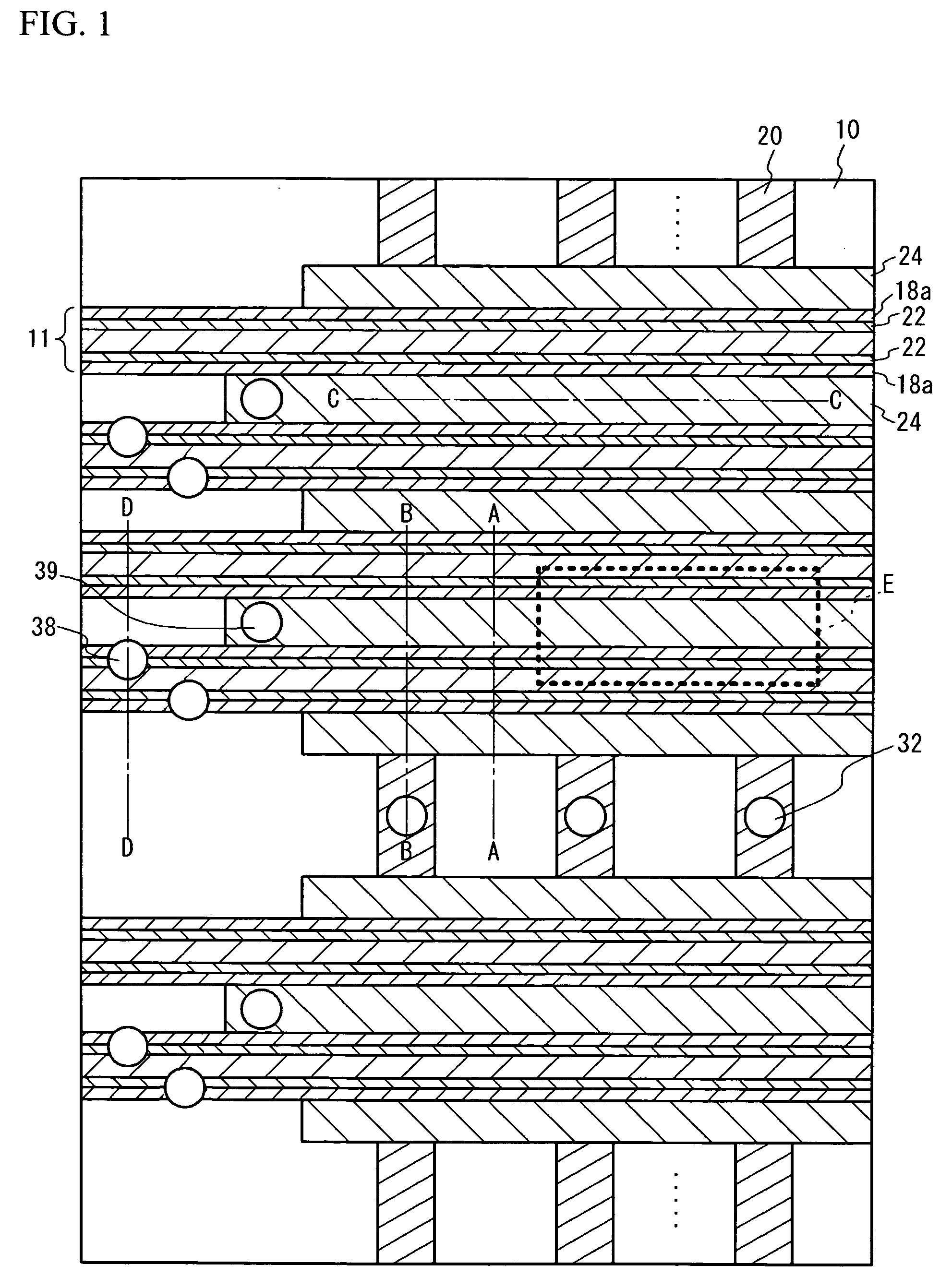
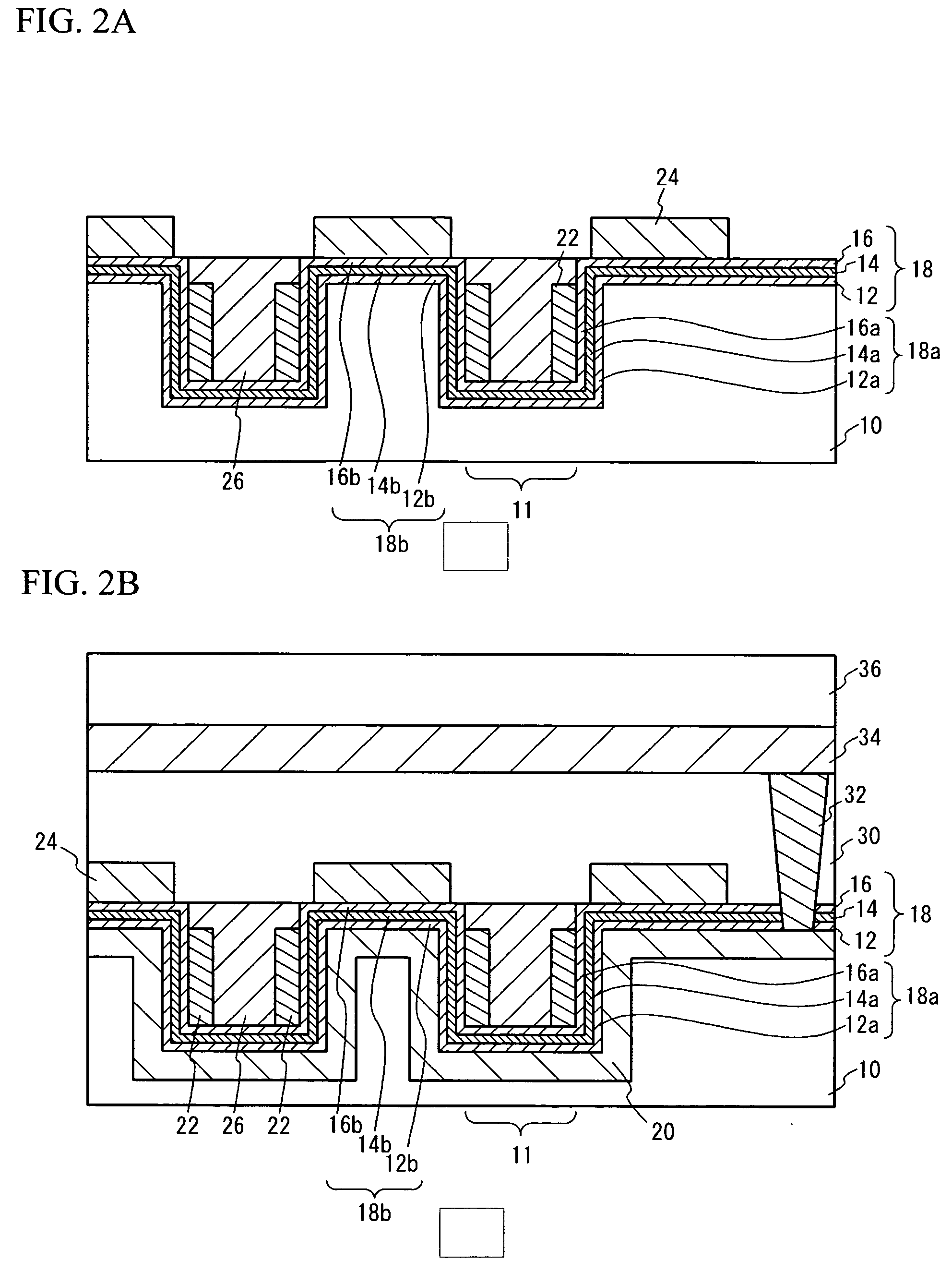
[0035]FIG. 1 is a top view of a memory cell region of a flash memory in accordance with a first embodiment of the present invention. In FIG. 1, a right-hand side is the memory cell region, and a left-hand side is a region in which word lines and a second wiring layer are connected. First and second interlayer insulation films 30 and 36 and first and second wiring layers 34 and 40 are not shown. Also, on the top and bottom of the drawing, only first and second word lines 22 and 24 and first and second ONO films 18a and 18b are not shown, but only bit lines 20 are shown. FIG. 2A is a cross-sectional view taken along the line A-A shown in FIG. 1, and FIG. 2B is a cross-sectional view taken along the line B-B shown in FIG. 1. FIG. 3A is a cross-sectional view taken along the line C-C shown in FIG. 1. FIG. 3B is a cross-sectional view taken along the line D-D shown in FIG. 1. Here, in FIG. 2A, the first and second wiring layers 34 and 40 and the first and second interlayer insulation fil...
second embodiment
[0051]FIG. 8 is a cross-sectional view of the flash memory taken along the line B-B shown in FIG. 1 in accordance with a second embodiment of the present invention. The trap layer 14a of a first ONO film 18a is physically isolated from the trap layer 14b of a second ONO film 18b. Other configurations are same as those of FIG. 2B in accordance with the first embodiment, and the same components and configurations as those shown in FIG. 2B have the same reference numerals and a detailed explanation will be omitted.
[0052] Next, a fabrication method of the flash memory employed in the second embodiment will be described, with reference to FIG. 9A through FIG. 10B. FIG. 9A through FIG. 10B are cross-sectional views taken along the line A-A shown in FIG. 1. Referring to FIG. 9A, a silicon oxide film is formed on the semiconductor substrate 10 as a tunnel oxide film 12b by, for example, a thermal oxidation process. A silicon nitride film is deposited on the tunnel oxide film 12b as the tra...
third embodiment
[0057] A third embodiment is an example of the fabrication method in which the protection layer is formed when the first word lines 22 are formed. A description will be given of the fabrication method of the flash memory employed in the third embodiment, with reference to FIG. 11A through FIG. 12C. FIG. 11A through FIG. 12C are cross-sectional views taken along the line A-A shown in FIG. 1. Referring to FIG. 11A, in a similar fabrication process as shown in FIG. 5A through FIG. 6A shown in accordance with the first embodiment, the polysilicon film 21 (the layer to be the first word lines 22) is formed on the side surfaces of the first ONO films 18a and on a top surface of the second ONO film 18b. Referring to FIG. 11B, a protection film 27 is applied in the trenches 11 and onto the polysilicon film 21 between the trenches 11. A resin such ad Hydrogen-Silsesquioxane (HSQ) or the like is employed for the protection film 27. Referring to FIG. 11C, the protection layer 27 between the tr...
PUM
 Abstract
Description
Claims
Application Information
 - R&D
- Intellectual Property
- Life Sciences
- Materials
- Tech Scout
- Unparalleled Data Quality
- Higher Quality Content
- 60% Fewer Hallucinations
Browse by: Latest US Patents, China's latest patents, Technical Efficacy Thesaurus, Application Domain, Technology Topic, Popular Technical Reports.
© 2025 PatSnap. All rights reserved.Legal|Privacy policy|Modern Slavery Act Transparency Statement|Sitemap|About US| Contact US: help@patsnap.com


